|
|
|
PDF HIP9011 Data sheet ( Hoja de datos )
| Número de pieza | HIP9011 | |
| Descripción | Engine Knock Signal Processor | |
| Fabricantes | Intersil Corporation | |
| Logotipo | ||
Hay una vista previa y un enlace de descarga de HIP9011 (archivo pdf) en la parte inferior de esta página. Total 11 Páginas | ||
|
No Preview Available !
®
Data Sheet
January 6, 2006
HIP9011
FN4367.2
Engine Knock Signal Processor
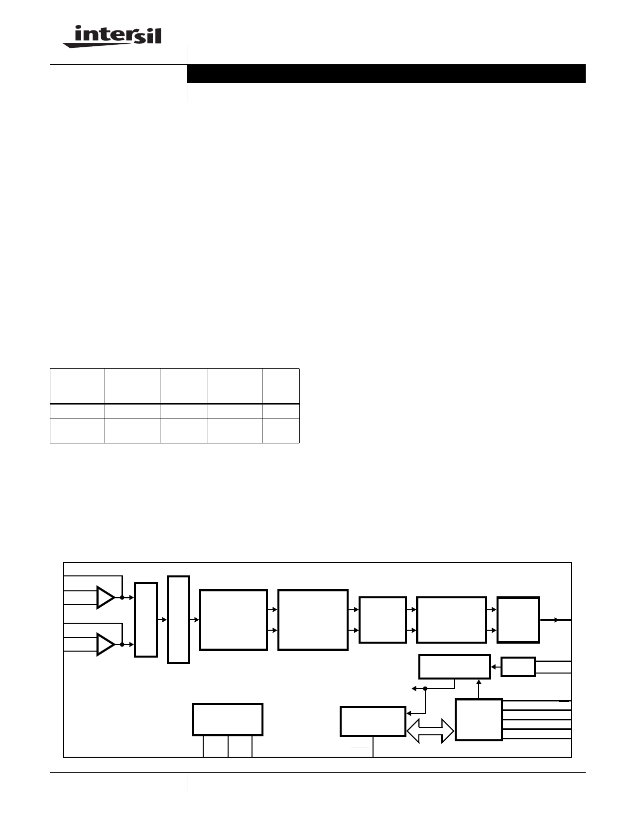
The HIP9011 is used to provide a method of detecting
premature detonation often referred to as “Knock or Ping” in
internal combustion engines.
The IC is shown in the Simplified Block Diagram. The chip
can select between one of two sensors, if needed for
accurate monitoring or for “V” type engines. Internal control
via the SPI bus is fast enough to switch sensors between
each firing cycle. A programmable bandpass filter
processes the signal from either of the sensor inputs. The
bandpass filter can be selected to optimize the extraction
the engine knock or ping signals from the engine
background noise. Further single processing is obtained by
full wave rectification of the filtered signal and applying it to
an integrator whose output voltage level is proportional to
the knock signal amplitude. The chip is under
microprocessor control via a SPI interface bus.
Ordering Information
PART
NUMBER
PART
MARKING
TEMP.
RANGE
(oC)
PKG.
PACKAGE DWG. #
HIP9011AB HIP9011AB -40 to 125 20 Ld SOIC M20.3
HIP9011ABZ HIP9011ABZ -40 to 125 20 Ld SOIC M20.3
(See Note)
(Pb-free)
Add “T” suffix for tape and reel.
NOTE: Intersil Pb-free plus anneal products employ special Pb-free
material sets; molding compounds/die attach materials and 100%
matte tin plate termination finish, which are RoHS compliant and
compatible with both SnPb and Pb-free soldering operations. Intersil
Pb-free products are MSL classified at Pb-free peak reflow
temperatures that meet or exceed the Pb-free requirements of
IPC/JEDEC J STD-020.
Simplified Block Diagram
Features
• Two Sensor Inputs
• Microprocessor Programmable
• Accurate and Stable Filter Elements
• Digitally Programmable Gain
• Digitally Programmable Time Constants
• Digitally Programmable Filter Characteristics
• On-Chip Crystal Oscillator
• Programmable Frequency Divider
• External Clock Frequencies up to 24MHz
- 4, 5, 6, 8, 10, 12, 16, 20, and 24MHz
• Operating Temperature Range -40oC to 125oC
• Pb-Free Plus Anneal Available (RoHS Compliant)
Applications
• Engine Knock Detector Processor
• Analog Signal Processing Where Controllable Filter
Characteristics are Required
CH0FB
CH0IN
-
CH0NI +
CH1FB
CH1IN
-
CH1NI +
PROGRAMMABLE
GAIN
STAGE
2- 0.111
64 STEPS
POWER SUPPLY
AND
BIAS CIRCUITS
VMID VDD GND
PROGRAMMABLE
BANDPASS
FILTER
1-20kHz
64 STEPS
ACTIVE
FULL WAVE
RECTIFIER
PROGRAMMABLE
INTEGRATOR
40 - 600µs
32 STEPS
OUTPUT
DRIVER INTOUT
AND
SAMPLE
AND HOLD
TO SWITCHED
CAPACITOR
NETWORKS
REGISTERS
AND
STATE MACHINE
TEST
PROGRAMMABLE
DIVIDER
OSCIN
CLOCK OSCOUT
SPI
INTERFACE
SCK
CS
SI
SO
INT/HOLD
1
CAUTION: These devices are sensitive to electrostatic discharge; follow proper IC Handling Procedures.
1-888-INTERSIL or 1-888-468-3774 | Intersil (and design) is a registered trademark of Intersil Americas Inc.
Copyright Intersil Americas Inc. 1999, 2006. All Rights Reserved
All other trademarks mentioned are the property of their respective owners.
1 page 
Timing Diagrams
HIP9011
INT/HOLD
CS
tCSCH
SCK
tCSH
tPWL
tCIH
tSCCH
tCSCF
SI
tSUH
SO
tPWH
B7 B6 B5 B4 B3 B2 B1 B0
tHH
B7 B6 B5 B4 B3 B2 B1 B0
FIGURE 1. SPI TIMING
SYMBOL
tCSCH
tCSCF
tPWL
tPWH
tSCCH
tSUH
tSUL
tHH
tHL
tCIH
tCSH
TABLE 1. SPI TIMING REQUIREMENTS
REQUIREMENT
Minimum time from CS falling edge to SCK rising edge.
Minimum time from CS falling edge to SCK falling edge.
Minimum time for the SCK low.
Minimum time for the SCK high.
Minimum time from SCK falling after 8 bits to CS raising edge.
Minimum time from data high to falling edge of spiclk.
Minimum time from data low to falling edge of spiclk.
Minimum time for data high after the falling edge of the spiclk.
Minimum time for data low after the falling edge of the spiclk.
Minimum time after CS raises until INT/HOLD goes high.
Minimum time between programming 2 internal registers.
t1
INT/HOLD
t2
INTOUT
t3
t4
SYMBOL
t1
t2
t3
t4
FIGURE 2. INTEGRATOR TIMING
TABLE 2. INTEGRATE/HOLD TIMING REQUIREMENTS
REQUIREMENT
Maximum rise time of the INT/HOLD signal.
Maximum time after INT/HOLD rises for INTOUT to begin to integrate.
Maximum fall time of INT/HOLD signal.
Typical time after INT/HOLD goes low before chip goes into hold state.
5
TIME
10ns
80ns
60ns
60ns
80ns
20ns
20ns
10ns
10ns
8µs
200ns
TIME
45ns
20µs
45ns
20µs
FN4367.2
January 6, 2006
5 Page 
HIP9011
Small Outline Plastic Packages (SOIC)
N
INDEX
AREA
E
-B-
H
0.25(0.010) M B M
123
-A-
D
SEATING PLANE
A
L
h x 45°
-C-
e A1
B
0.25(0.010) M C A M B S
α
0.10(0.004)
C
NOTES:
1. Symbols are defined in the “MO Series Symbol List” in Section
2.2 of Publication Number 95.
2. Dimensioning and tolerancing per ANSI Y14.5M-1982.
3. Dimension “D” does not include mold flash, protrusions or gate
burrs. Mold flash, protrusion and gate burrs shall not exceed
0.15mm (0.006 inch) per side.
4. Dimension “E” does not include interlead flash or protrusions.
Interlead flash and protrusions shall not exceed 0.25mm (0.010
inch) per side.
5. The chamfer on the body is optional. If it is not present, a visual
index feature must be located within the crosshatched area.
6. “L” is the length of terminal for soldering to a substrate.
7. “N” is the number of terminal positions.
8. Terminal numbers are shown for reference only.
9. The lead width “B”, as measured 0.36mm (0.014 inch) or greater
above the seating plane, shall not exceed a maximum value of
0.61mm (0.024 inch)
10. Controlling dimension: MILLIMETER. Converted inch
dimensions are not necessarily exact.
M20.3 (JEDEC MS-013-AC ISSUE C)
20 LEAD WIDE BODY SMALL OUTLINE PLASTIC PACKAGE
INCHES
MILLIMETERS
SYMBOL MIN MAX MIN MAX NOTES
A
0.0926 0.1043 2.35
2.65
-
A1
0.0040 0.0118 0.10
0.30
-
B
0.014
0.019
0.35
0.49
9
C
0.0091 0.0125 0.23
0.32
-
D
0.4961 0.5118 12.60
13.00
3
E
0.2914 0.2992 7.40
7.60
4
e 0.050 BSC
1.27 BSC
-
H
0.394
0.419 10.00
10.65
-
h
0.010
0.029
0.25
0.75
5
L
0.016
0.050
0.40
1.27
6
N 20
20 7
α 0° 8° 0° 8° -
Rev. 2 6/05
All Intersil U.S. products are manufactured, assembled and tested utilizing ISO9000 quality systems.
Intersil Corporation’s quality certifications can be viewed at www.intersil.com/design/quality
Intersil products are sold by description only. Intersil Corporation reserves the right to make changes in circuit design, software and/or specifications at any time without
notice. Accordingly, the reader is cautioned to verify that data sheets are current before placing orders. Information furnished by Intersil is believed to be accurate and
reliable. However, no responsibility is assumed by Intersil or its subsidiaries for its use; nor for any infringements of patents or other rights of third parties which may result
from its use. No license is granted by implication or otherwise under any patent or patent rights of Intersil or its subsidiaries.
For information regarding Intersil Corporation and its products, see www.intersil.com
11 FN4367.2
January 6, 2006
11 Page | ||
| Páginas | Total 11 Páginas | |
| PDF Descargar | [ Datasheet HIP9011.PDF ] | |
Hoja de datos destacado
| Número de pieza | Descripción | Fabricantes |
| HIP9010 | Engine Knock Signal Processor | Intersil Corporation |
| HIP9010AB | Engine Knock Signal Processor | Intersil Corporation |
| HIP9011 | Engine Knock Signal Processor | Intersil Corporation |
| Número de pieza | Descripción | Fabricantes |
| SLA6805M | High Voltage 3 phase Motor Driver IC. |
Sanken |
| SDC1742 | 12- and 14-Bit Hybrid Synchro / Resolver-to-Digital Converters. |
Analog Devices |
|
DataSheet.es es una pagina web que funciona como un repositorio de manuales o hoja de datos de muchos de los productos más populares, |
| DataSheet.es | 2020 | Privacy Policy | Contacto | Buscar |