|
|
|
PDF HIP9010 Data sheet ( Hoja de datos )
| Número de pieza | HIP9010 | |
| Descripción | Engine Knock Signal Processor | |
| Fabricantes | Intersil Corporation | |
| Logotipo | ||
Hay una vista previa y un enlace de descarga de HIP9010 (archivo pdf) en la parte inferior de esta página. Total 12 Páginas | ||
|
No Preview Available !
Data Sheet
HIP9010
November 1998 File Number 3601.4
Engine Knock Signal Processor
The HIP9010 is used to provide a method of detecting
premature detonation or “Knock” in automotive engines.
A block diagram of this IC is shown in Figure 1. The chip
alternately selects one of the two sensors mounted on the
engine block. Two programmable bandpass filters process
the signal from both sensors, and divides the signal into two
channels. When the engine is not knocking, programmable
gain adjust stages are set to ensure that both the reference
channel and the knock channel contain similar energies.
This technique ensures that the detection system is
comparatively immune to changes in the engine background
noise level. When the engine is knocking, the energy in the
knock channel increases.
Ordering Information
TEMP.
PART NUMBER RANGE (oC)
PACKAGE
HIP9010AB
-40 to 125 20 Ld SOIC (W)
PKG.
NO.
M20.3
Features
• Two Sensor Inputs
• Microprocessor Programmable
• Accurate and Stable Filter Elements
• Digitally Programmable Gain
• Digitally Programmable Time Constants
• Digitally Programmable Filter Characteristics
• On-Chip Clock
• Operating Temperature Range -40oC to 125oC
Applications
• Engine Knock Detector Processor
• Analog Signal Processing where Controllable Filter
Characteristics are Required
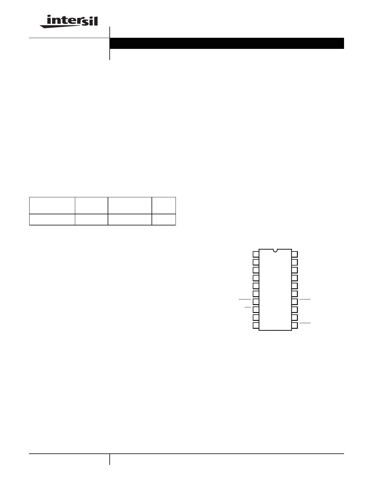
Pinout
HIP9010
(SOIC)
TOP VIEW
VDD
GND
VMID
INOUT
1
2
3
4
NC 5
NC 6
INT/HOLD 7
CS 8
OSCIN 9
OSCOUT 10
20 S0IN
19 S0FB
18 S1FB
17 S1IN
16 NC
15 NC
14 TEST
13 SCK
12 MOSI
11 MISO
4-1 CAUTION: These devices are sensitive to electrostatic discharge; follow proper IC Handling Procedures.
http://www.intersil.com or 407-727-9207 | Copyright © Intersil Corporation 1999
1 page 
HIP9010
TRANSDUCERS
+5V
C3, 0.022µF
C2, 3.3nF
R2
C1, 3.3nF
R4
R1
20pF R3
VDD
VMID
HIP9010
GND
S1IN
S1FB
S0IN
S0FB
OSCIN
MOSI
MISO
SCK
CS
INT/HOLD
TEST
4MHz
20pF
OSCOUT INTOUT
1M
SPI BUS
A/D
CONVERTER
MICROPROCESSOR
FIGURE 2. SIMPLIFIED BLOCK DIAGRAM OF THE HIP9010 IN AN AUTOMOTIVE APPLICATION
Pin Descriptions
PIN
NUMBER
SYMBOL
1 VDD
2 GND
3 VMID
4
5 and 6
7
8
9
INTOUT
NC
INT/HOLD
CS
OSCIN
10 OSCOUT
11 MISO
12
13
14
15 and 16
17
MOSI
SCK
TEST
NC
S1IN
18 S1FB
19 S0FB
20 S0IN
DESCRIPTION
5V power input.
This terminal is tied to ground.
This terminal is tied to the internal mid-supply generator and is brought out for supply bypassing by a 0.022µF
capacitor.
Buffered output of the integrator.
These terminals are not internally connected. DO NOT USE.
Selects whether the chip is in the Integrate Mode (Input High) or in the Hold Mode (Input Low).
A low input on this pin enables the chip to communicate over the SPI bus.
Input to inverter used for the oscillator circuit. A 4MHz crystal or ceramic resonator is connected between this
pin and pin 10. To bias the inverter, a 1.0MΩ to 10MΩ resistor is usually connected between this pin and pin 10.
Output of the inverter used for the oscillator. See pin 9 above.
Output of the chip SPI data bus. It is the inversion of the chip DATAIN line. This is an open drain output. The
output must be disabled by placing the CS High when the chip is not selected.
Input of the chip SPI data bus. Data length is eight bits.
Input from the SPI clock. Normally high, the data is clocked to the chip internal circuitry on the rising clock edge.
A low on this pin places the chip in the test mode. For normal operation this terminal is tied high or left open.
These terminals are not internally connected. DO NOT USE.
Inverting input to sensor one amplifier. A resistor is tied from this summing input to the transducer. A second
resistor is tied between this terminal and terminal 18, S1FB to establish the gain of the amplifier.
Output of the sensor one amplifier. This terminal is used to apply feedback.
Output of the sensor zero amplifier. This terminal is used to apply feedback.
Inverting input to sensor zero amplifier. A resistor is tied from this summing input to the transducer. A second
resistor is tied between this terminal and terminal 19, S0FB to establish the gain of the amplifier.
4-5
5 Page 
CS
INT/HOLD
FIGURE 7. POWER UP SEQUENCE
T1
INT/HOLD
T2
INTOUT
T3
T4
HIP9010
Test Multiplexer
This circuit receives the positive and negative outputs out of
the two integrators, together with the outputs from different
parts of the chip. The output is controlled by the fifth
programming word of the communications protocol. This
multiplexes the switch capacitor filter output, the gain control
output as well as the antialias output.
Differential to Single-ended Converter
This signal takes the output of the two integrators (through
the test multiplexer circuit) and provides a signal that is the
sum of the two signals. This technique is used to improve the
noise immunity of the system.
Output Buffer
This output amplifier is the same as the input amplifier used
to interface to the sensors. For test purposes when we look
at the output of the antialias filter, the input amplifiers are in
the power down mode.
FIGURE 8. INTEGRATOR TIMING
TABLE 4. INTERGRATE/HOLD TIMING REQUIREMENTS
DESCRIPTION
UNITS
T1 maximum rise time of the INT/HOLD signal.
45ns
T2 maximum time after INT/HOLD rises for the INOUT to 20µs
begin to intergrate.
T3 maximum fall time of INT/HOLD signal.
45ns
T4 typical time after INT/HOLD goes low before chip
goes into hold state.
20µs
T5 minimum INT/HOLD time during power up sequence. 1µs
4-11
11 Page | ||
| Páginas | Total 12 Páginas | |
| PDF Descargar | [ Datasheet HIP9010.PDF ] | |
Hoja de datos destacado
| Número de pieza | Descripción | Fabricantes |
| HIP9010 | Engine Knock Signal Processor | Intersil Corporation |
| HIP9010AB | Engine Knock Signal Processor | Intersil Corporation |
| HIP9011 | Engine Knock Signal Processor | Intersil Corporation |
| Número de pieza | Descripción | Fabricantes |
| SLA6805M | High Voltage 3 phase Motor Driver IC. |
Sanken |
| SDC1742 | 12- and 14-Bit Hybrid Synchro / Resolver-to-Digital Converters. |
Analog Devices |
|
DataSheet.es es una pagina web que funciona como un repositorio de manuales o hoja de datos de muchos de los productos más populares, |
| DataSheet.es | 2020 | Privacy Policy | Contacto | Buscar |