|
|
|
PDF 07XSC200 Data sheet ( Hoja de datos )
| Número de pieza | 07XSC200 | |
| Descripción | Dual High Side Switch | |
| Fabricantes | Freescale Semiconductor | |
| Logotipo | ||
Hay una vista previa y un enlace de descarga de 07XSC200 (archivo pdf) en la parte inferior de esta página. Total 30 Páginas | ||
|
No Preview Available !
Freescale Semiconductor
Advance Information
Document Number: MC07XSC200
Rev. 2.0, 9/2013
Dual High Side Switch
(7.0 mOhm)
07XSC200
The 07XSC200 is one in a family of devices designed for low-voltage
lighting or factory automation applications. Its two low RDS(ON)
MOSFETs (dual 7.0 m) can control two separate 55 W / 28 W bulbs,
and/or Xenon modules, and/or LEDs, and/or DC low voltage motors.
Programming, control and diagnostics are accomplished using a 16-bit
SPI interface. Its output with selectable slew rate improves
electromagnetic compatibility (EMC) behavior. Additionally, each
output has its own parallel input or SPI control for pulse-width
modulation (PWM) control if desired. The 07XSC200 allows the user to
program via the SPI, the fault current trip levels and duration of
acceptable inrush. The device has Fail-safe mode to provide fail-safe
functionality of the outputs in case of MCU damaged.
The 07XSC200 is packaged in a Pb-free power-enhanced 32 pins
SOIC package with exposed tab.
This device is powered by SMARTMOS technology.
Features
• Dual 7.0 m max high side switch (at 25 °C)
• Operating voltage range of 6.0 to 20 V with sleep current < 5.0 µA,
extended mode from 4.0 to 28 V
• 8.0 MHz 16-bit 3.3 V and 5.0 V SPI control and status reporting with
daisy chain capability
• PWM module using external clock or calibratable internal oscillator
with programmable outputs delay management
• Smart overcurrent shutdown compliant to huge inrush current,
severe short-circuit, overtemperature protections with time limited
auto-retry, and Fail-safe mode, in case of MCU damage
• Output OFF or ON OpenLoad detection compliant to bulbs or LEDs
and short to battery detection. Analog current feedback with
selectable ratio and board temperature feedback.
HIGH SIDE SWITCH
EK SUFFIX PB-FREE
98ASA00368D
32-PIN EXPOSED PAD SOIC
ORDERING INFORMATION
Device
Temperature
Range (TA)
Package
MC07XSC200EK
-40 to 125 °C
32 SOIC
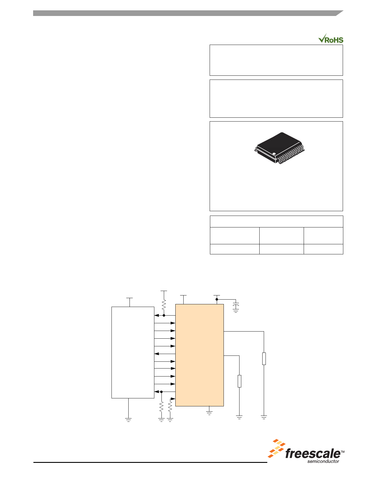
VDD
VDD
MCU
I/O
I/O
SO
SCLK
CSB
SI
I/O
I/O
I/O
I/O
A/D
VDD
VPWR
07XSC200
VDD
VPWR
FSB
WAKE
SI
SCLK
HS1
CSB
SO
RSTB
CLOCK
HS0
IN0
IN1
CSNS
FSI GND
GND
LOAD
LOAD
Figure 1. 07XSC200 Simplified Application Diagram
* This document contains certain information on a new product.
Specifications and information herein are subject to change without notice.
© Freescale Semiconductor, Inc., 2013. All rights reserved.
Free Datasheet http://www.datasheet4u.com/
1 page 
3 Electrical Characteristics
3.1 Maximum Ratings
Table 2. Maximum Ratings
All voltages are with respect to ground unless otherwise noted. Exceeding these ratings may cause a malfunction or permanent
damage to the device.
Ratings
Symbol
Value
Unit
ELECTRICAL RATINGS
VPWR Supply Voltage Range
• Load Dump at 25 °C (400 ms)
• Maximum Operating Voltage
• Reverse Battery
VPWR(SS)
41
28
-18
V
VDD Supply Voltage Range
Input/Output Voltage
WAKE Input Clamp Current
CSNS Input Clamp Current
HS [0:1] Voltage
• Positive
• Negative
VDD
(4)
ICL(WAKE)
ICL(CSNS)
VHS[0:1]
-0.3 to 5.5
-0.3 to VDD+0.3
2.5
2.5
41
-24
V
V
mA
mA
V
Output Current per Channel
• Nominal Continuous Current(1)
• Short-circuit Transient Current
• Reverse Continuous Current(1)
IHS[0:1]
26
116
-26
A
High Side Breakdown Voltage
HS[0,1] Output Clamp Energy using single pulse method(2)
ESD Voltage(3)
• Human Body Model (HBM) for HS[0:1], VPWR and GND
• Human Body Model (HBM) for other pins
• Charge Device Model (CDM)
Corner Pins (1, 27, 28, 57)
All Other Pins
VPWR - VHS
ECL [0:1]
VESD1
VESD2
VESD3
VESD4
47
100
± 8000
± 2000
± 750
± 500
V
mJ
V
Notes
1. Continuous high side output current rating so long as maximum junction temperature is not exceeded. Calculation of maximum output
current using board thermal resistance is required.
2. Active clamp energy using single-pulse method (L = 2.0 mH, RL = 0 , VPWR = 14 V, TJ = 150 C initial).
3. ESD testing is performed in accordance with the Human Body Model (HBM) (CZAP = 100 pF, RZAP = 1500 ), the Machine Model (MM)
(CZAP = 200 pF, RZAP = 0 ), and the Charge Device Model (CDM), Robotic (CZAP = 4.0 pF).
4. Input / Output pins are: IN[0:1], CLOCK, RSTB, FSI, CSNS, SI, SCLK, CSB, SO, FSB
Analog Integrated Circuit Device Data
Freescale Semiconductor
07XSC200
5
Free Datasheet http://www.datasheet4u.com/
5 Page 
Table 3. Static Electrical Characteristics (continued)
Characteristics noted under conditions 6.0 V VPWR 20 V, 3.0 V VDD 5.5 V, -40 C TA 125 C, GND = 0 V, unless
otherwise noted. Typical values noted reflect the approximate parameter means at TA = 25 °C under nominal conditions, unless
otherwise noted.
Characteristic
Symbol
Min Typ Max Unit
CONTROL INTERFACE
Input Logic High Voltage(19)
Input Logic Low Voltage(19)
Input Logic Pull-down Current (SCLK, SI)(22)
Input Logic Pull-up Current (CSB) (23)
SO, FSB Tri-state Capacitance(20)
Input Logic Pull-down Resistor (RSTB, WAKE, CLOCk and IN[0:1])
Input Capacitance(20)
Wake Input Clamp Voltage(21)
• ICL(WAKE) < 2.5 mA
VIH
VIL
IDWN
IUP
CSO
RDWN
CIN
VCL(WAKE)
2.0
-0.3
5.0
5.0
–
125
–
18
– VDD+0.3 V
– 0.8 V
– 20 A
– 20 A
– 20 pF
250 500 k
4.0 12 pF
V
25 32
Wake Input Forward Voltage
• ICL(WAKE) = -2.5 mA
VF(WAKE)
V
-2.0 – -0.3
SO High-state Output Voltage
• IOH = 1.0 mA
SO and FSB Low-state Output Voltage
• IOL = -1.0 mA
VSOH
V
VDD-0.4
–
–
VSOL
V
– – 0.4
SO, CSNS and FSB Tri-state Leakage Current
• CSB = VIH and 0 V < VSO < VDD, or FSB = 5.5 V, or CSNS = 0.0 V
FSI External Pull-down Resistance(24)
• Watchdog Disabled
• Watchdog Enabled
ISO(LEAK)
RFS
-2.0 0.0 2.0
– 0.0 1.0
10 Infinite
–
A
k
Notes
19. Upper and lower logic threshold voltage range applies to SI, CSB, SCLK, FSB, IN[0:1], CLOCK and WAKE input signals. The WAKE and
RSTB signals may be supplied by a derived voltage referenced to VPWR.
20. Input capacitance of SI, CSB, SCLK, RSTB, IN[0:1], CLOCK and WAKE. This parameter is guaranteed by process monitoring but is not
production tested.
21. The current must be limited by a series resistance when using voltages > 7.0 V.
22. Pull-down current is with VSI > 1.0 V and VSCLK > 1.0 V.
23. Pull-up current is with VCSB < 2.0 V. CSB has an active internal pull-up to VDD.
24. In Fail-safe HS[0:1] depends respectively on IN[0:1]. FSI has an active internal pull-up to VREG ~ 3.0 V.
Analog Integrated Circuit Device Data
Freescale Semiconductor
07XSC200
11
Free Datasheet http://www.datasheet4u.com/
11 Page | ||
| Páginas | Total 30 Páginas | |
| PDF Descargar | [ Datasheet 07XSC200.PDF ] | |
Hoja de datos destacado
| Número de pieza | Descripción | Fabricantes |
| 07XSC200 | Dual High Side Switch | Freescale Semiconductor |
| Número de pieza | Descripción | Fabricantes |
| SLA6805M | High Voltage 3 phase Motor Driver IC. |
Sanken |
| SDC1742 | 12- and 14-Bit Hybrid Synchro / Resolver-to-Digital Converters. |
Analog Devices |
|
DataSheet.es es una pagina web que funciona como un repositorio de manuales o hoja de datos de muchos de los productos más populares, |
| DataSheet.es | 2020 | Privacy Policy | Contacto | Buscar |