|
|
|
PDF CAT93C66 Data sheet ( Hoja de datos )
| Número de pieza | CAT93C66 | |
| Descripción | 4 kb Microwire Serial CMOSEEPROM | |
| Fabricantes | ON Semiconductor | |
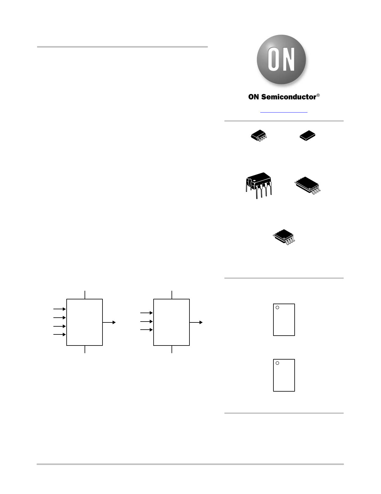
| Logotipo | ||
Hay una vista previa y un enlace de descarga de CAT93C66 (archivo pdf) en la parte inferior de esta página. Total 13 Páginas | ||
|
No Preview Available !
CAT93C66, CAT93W66
4 kb Microwire Serial CMOS
EEPROM
Description
The CAT93C66 is a 4 kb CMOS Serial EEPROM device which is
organized as either 256 registers of 16 bits (ORG pin at VCC) or 512
registers of 8 bits (ORG pin at GND). The CAT93W66 features x16
memory organization only. Each register can be written (or read)
serially by using the DI (or DO) pin. The device features sequential
read and self−timed internal write with auto−clear. On−chip
Power−On Reset circuitry protects the internal logic against powering
up in the wrong state.
Features
• High Speed Operation: 2 MHz
• 1.8 V to 5.5 V Supply Voltage Range
• Selectable x8 or x16 Memory Organization: CAT93C66
• Sequential Read
• Software Write Protection
• Power−up Inadvertent Write Protection
• Low Power CMOS Technology
• 1,000,000 Program/Erase Cycles
• 100 Year Data Retention
• Industrial and Extended Temperature Ranges
• 8−lead PDIP, SOIC, TSSOP and 8−pad TDFN Packages
• These Devices are Pb−Free, Halogen Free/BFR Free, and RoHS
Compliant
VCC
VCC
ORG
CS
SK
DI
CAT93C66
CS
DO SK
DI
CAT93W66
DO
GND
GND
Figure 1. Functional Symbols
CAT93C66 Selectable Organization:
When the ORG pin is connected to VCC, the x16 organization is
selected. When it is connected to ground, the x8 organization is
selected. If the ORG pin is left unconnected, then an internal pull−up
device will select the x16 organization.
CAT93W66*:
The device works in x16 mode only.
*Not recommended for new designs
www.onsemi.com
SOIC−8
V SUFFIX
CASE 751BD
TDFN−8
VP2 SUFFIX
CASE 511AK
PDIP−8
L SUFFIX
CASE 646AA
TSSOP−8
Y SUFFIX
CASE 948AL
SOIC−8
X SUFFIX
CASE 751BE
PIN CONFIGURATION
(Top View)
CS 1
SK 2
DI 3
DO 4
8 VCC
7 NC
6 ORG
5 GND
PDIP (L), SOIC (V, X),
TSSOP (Y),
TDFN (VP2)
CS 1
SK 2
DI 3
DO 4
8 VCC
7 NC
6 NC
5 GND
TDFN (VP2)
CAT93W66*
ORDERING INFORMATION
See detailed ordering and shipping information in the package
dimensions section on page 13 of this data sheet.
© Semiconductor Components Industries, LLC, 2015
August, 2015 − Rev. 13
1
Publication Order Number:
CAT93C66/D
1 page 
CAT93C66, CAT93W66
Read
Upon receiving a READ command and an address
(clocked into the DI pin), the DO pin of the CAT93C66,
CAT93W66 will come out of the high impedance state and,
after sending an initial dummy zero bit, will begin shifting
out the data addressed (MSB first). The output data bits will
toggle on the rising edge of the SK clock and are stable after
the specified time delay (tPD0 or tPD1).
For the CAT93C66, CAT93W66 after the initial data word
has been shifted out and CS remains asserted with the SK
clock continuing to toggle, the device will automatically
increment to the next address and shift out the next data word
in a sequential READ mode. As long as CS is continuously
asserted and SK continues to toggle, the device will keep
incrementing to the next address automatically until it
reaches to the end of the address space, then loops back to
address 0. In the sequential READ mode, only the initial data
word is preceeded by a dummy zero bit. All subsequent data
words will follow without a dummy zero bit. The READ
instruction timing is illustrated in Figure 3.
Erase/Write Enable and Disable
The device powers up in the write disable state. Any
writing after power−up or after an EWDS (erase/write
disable) instruction must first be preceded by the EWEN
(erase/write enable) instruction. Once the write instruction
is enabled, it will remain enabled until power to the device
is removed, or the EWDS instruction is sent. The EWDS
instruction can be used to disable all CAT93C66,
CAT93W66 write and erase instructions, and will prevent
any accidental writing or clearing of the device. Data can be
read normally from the device regardless of the write
enable/disable status. The EWEN and EWDS instructions
timing is shown in Figure 4.
tSKHI
tSKLOW
tCSH
SK
tDIS
DI VALID
tCSS
CS
VALID
tDIH
tDIS
tPD0, tPD1
tCSMIN
DO DATA VALID
Figure 2. Synchronous Data Timing
SK
CS
AN AN−1
DI 1 1 0
A0
tPD0
HIGH−Z
DO
Don’t Care
Dummy 0
D15 . . . D0
or
D7 . . . D0
Address + 1
D15 . . . D0
or
D7 . . . D0
Address + 2
D15 . . . D0
or
D7 . . . D0
Address + n
D15 . . .
or
D7 . . .
Figure 3. READ Instruction Timing
www.onsemi.com
5
5 Page 
CAT93C66, CAT93W66
PACKAGE DIMENSIONS
TSSOP8, 4.4x3
CASE 948AL−01
ISSUE O
b
SYMBOL MIN
NOM
MAX
A 1.20
A1 0.05
0.15
A2 0.80 0.90 1.05
E1 E
b 0.19
0.30
c 0.09
0.20
D 2.90 3.00 3.10
E 6.30 6.40 6.50
E1 4.30 4.40 4.50
e 0.65 BSC
L 1.00 REF
L1 0.50 0.60 0.75
θ 0º
8º
e
TOP VIEW
D
A2
A
q1
c
SIDE VIEW
A1
Notes:
(1) All dimensions are in millimeters. Angles in degrees.
(2) Complies with JEDEC MO-153.
L1
END VIEW
L
www.onsemi.com
11
11 Page | ||
| Páginas | Total 13 Páginas | |
| PDF Descargar | [ Datasheet CAT93C66.PDF ] | |
Hoja de datos destacado
| Número de pieza | Descripción | Fabricantes |
| CAT93C66 | 1K/2K/2K/4K/16K-Bit Microwire Serial E2PROM | Catalyst Semiconductor |
| CAT93C66 | 4 kb Microwire Serial CMOSEEPROM | ON Semiconductor |
| CAT93C6611 | Supervisory Circuits with Microwire Serial CMOS E2PROM/ Precision Reset Controller and Watchdog Timer | Catalyst Semiconductor |
| CAT93C6612 | Supervisory Circuits with Microwire Serial CMOS E2PROM/ Precision Reset Controller and Watchdog Timer | Catalyst Semiconductor |
| Número de pieza | Descripción | Fabricantes |
| SLA6805M | High Voltage 3 phase Motor Driver IC. |
Sanken |
| SDC1742 | 12- and 14-Bit Hybrid Synchro / Resolver-to-Digital Converters. |
Analog Devices |
|
DataSheet.es es una pagina web que funciona como un repositorio de manuales o hoja de datos de muchos de los productos más populares, |
| DataSheet.es | 2020 | Privacy Policy | Contacto | Buscar |