|
|
|
PDF ADRF6850 Data sheet ( Hoja de datos )
| Número de pieza | ADRF6850 | |
| Descripción | 100 MHz to 1000 MHz Integrated Broadband Receiver | |
| Fabricantes | Analog Devices | |
| Logotipo | ||
Hay una vista previa y un enlace de descarga de ADRF6850 (archivo pdf) en la parte inferior de esta página. Total 30 Páginas | ||
|
No Preview Available !
FEATURES
IQ quadrature demodulator
Integrated fractional-N PLL and VCO
Gain control range: 60 dB
Input frequency range: 100 MHz to 1000 MHz
Input P1dB: +12 dBm at 0 dB gain
Input IP3: +22.5 dBm at 0 dB gain
Noise figure: 11 dB at >39 dB gain, 49 dB at 0 dB gain
Baseband 1 dB bandwidth: 250 MHz in wideband mode,
50 MHz in narrow-band mode
SPI/I2C serial interface
Power supply: +3.3 V/350 mA
APPLICATIONS
Broadband communications
Cellular communications
Satellite communications
100 MHz to 1000 MHz
Integrated Broadband Receiver
ADRF6850
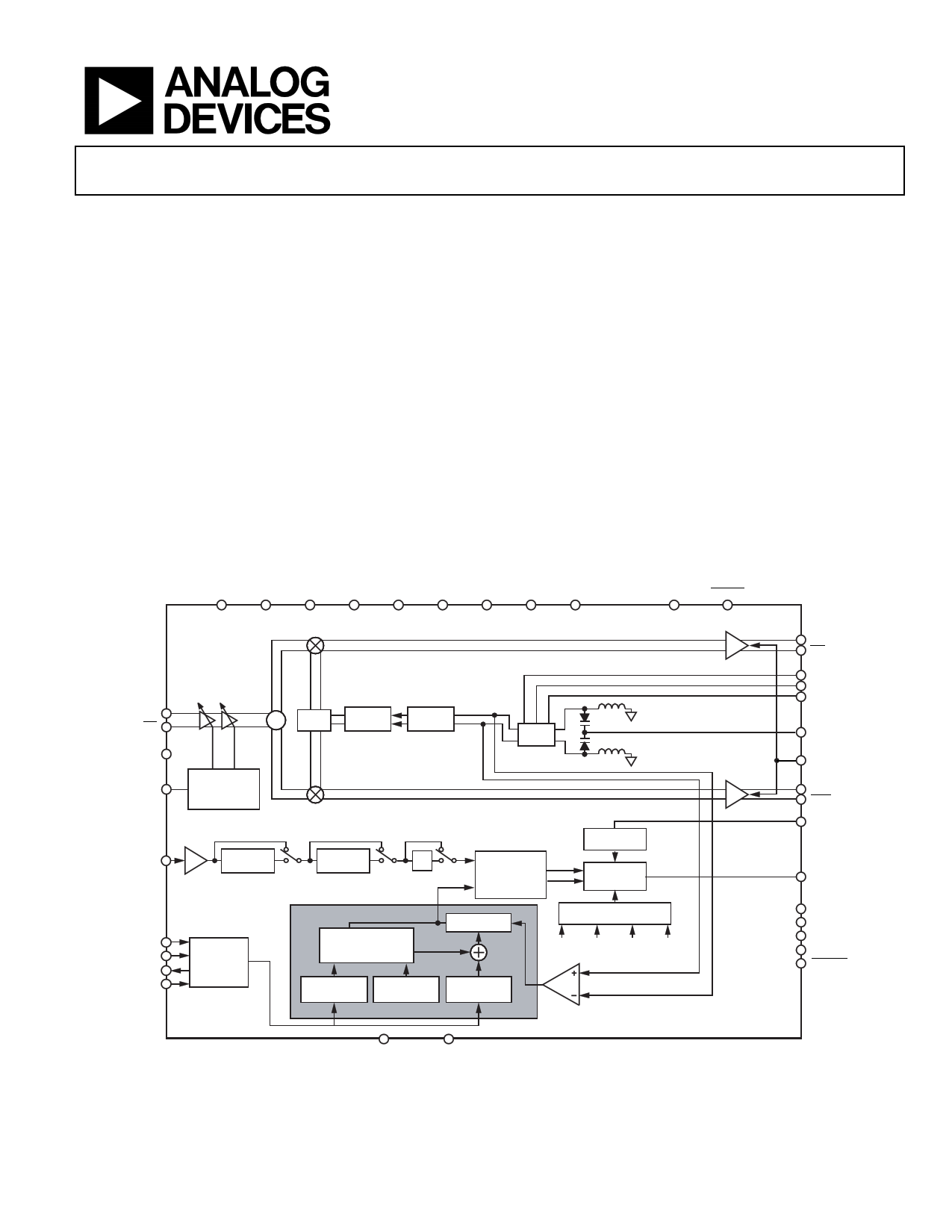
GENERAL DESCRIPTION
The ADRF6850 is a highly integrated broadband quadrature
demodulator, frequency synthesizer, and variable gain amplifier
(VGA). The device covers an operating frequency range from
100 MHz to 1000 MHz for use in both narrow-band and wideband
communications applications, performing quadrature demodu-
lation from IF directly to baseband frequencies.
The ADRF6850 demodulator includes a high modulus
fractional-N frequency synthesizer with integrated VCO,
providing better than 1 Hz frequency resolution, and a 60 dB
gain control range provided by a front-end VGA.
Control of all the on-chip registers is through a user-selected
SPI interface or I2C interface. The device operates from a single
power supply ranging from 3.15 V to 3.45 V.
VCC1
VCC2
VCC3
FUNCTIONAL BLOCK DIAGRAM
VCC4 VCC5 VCC6 VCC7 VCC8 VCC9
LOMON LOMON
60dB
GAIN CONTROL
RANGE
RFI
RFI
RFCM
VGAIN
SEQUENCED
GAIN
INTERFACE
0°/90°
DRIVER
RFDIV
VCO
CORE
REFIN
×2
DOUBLER
SDI/SDA
CLK/SCL
SDO
CS
SPI/
I2C
INTERFACE
ADRF6850
5-BIT
DIVIDER
÷2
THIRD-ORDER
FRACTIONAL
INTERPOLATOR
+ PHASE
FREQUENCY
– DETECTOR
REFERENCE
CHARGE
PUMP
N-COUNTER
CURRENT SETTING
RFCP4 RFCP3 RFCP2 RFCP1
FRACTIONAL MODULUS
REGISTER
225
INTEGER
REGISTER
GND
MUXOUT
Figure 1.
IBB
IBB
CCOMP1
CCOMP2
CCOMP3
VTUNE
VOCM
QBB
QBB
RSET
CP
LF3
LF2
LDET
TESTLO
TESTLO
Rev. 0
Information furnished by Analog Devices is believed to be accurate and reliable. However, no
responsibilityisassumedbyAnalogDevices for itsuse,nor foranyinfringementsofpatentsor other
rights of third parties that may result from its use. Specifications subject to change without notice. No
license is granted by implication or otherwise under any patent or patent rights of Analog Devices.
Trademarksandregisteredtrademarksarethepropertyoftheirrespectiveowners.
One Technology Way, P.O. Box 9106, Norwood, MA 02062-9106, U.S.A.
Tel: 781.329.4700
www.analog.com
Fax: 781.461.3113
©2010 Analog Devices, Inc. All rights reserved.
Free Datasheet http://www.datasheet4u.com/
1 page 
TIMING CHARACTERISTICS
I2C Interface Timing
Table 2.
Parameter1
SCL Clock Frequency
SCL Pulse Width High
SCL Pulse Width Low
Start Condition Hold Time
Start Condition Setup Time
Data Setup Time
Data Hold Time
Stop Condition Setup Time
Data Valid Time
Data Valid Acknowledge Time
Bus Free Time
1 See Figure 2.
Symbol
fSCL
tHIGH
tLOW
tHD;STA
tSU;STA
tSU;DAT
tHD;DAT
tSU;STO
tVD;DAT
tVD;ACK
tBUF
SDA
SCL
S
START
CONDITION
tSU;DAT
tHD;STA
tLOW
1/fSCL
tHD;DAT
ADRF6850
Limit
400
600
1300
600
600
100
300
600
900
900
1300
ttVVDD;;DAACTK
AND
(ACK
SIGNAL
ONLY)
tSU;STA
tSU;STO
Unit
kHz max
ns min
ns min
ns min
ns min
ns min
ns min
ns min
ns max
ns max
ns min
tBUF
tHIGH
S
Figure 2. I2C Port Timing Diagram
P
STOP
CONDITION
S
Rev. 0 | Page 5 of 36
Free Datasheet http://www.datasheet4u.com/
5 Page 
20
RF = 100MHz
RF = 300MHz
10 RF = 550MHz
RF = 800MHz
RF = 1000MHz
0
–10
–20
–30
–40
–50
–60
–10 0
10 20 30 40 50 60 70
CHANNEL GAIN (dB)
Figure 11. Input 1dB Compression Point (IP1dB) vs. Channel Gain, and RF
Input Frequency, VOCM = 1.6 V, Nominal Conditions, Narrow-Band Mode
20
IQ = 20MHz
IQ = 50MHz
10
IQ = 100MHz
0 IQ = 200MHz
IQ = 250MHz
–10
–20
–30
–40
–50
–60
0
10 20 30 40 50 60
CHANNE L GAIN (dB)
Figure 12. Input 1dB Compression Point (IP1dB) vs. Channel Gain, and IQ
Output Frequency, LO = 1000 MHz, Nominal Conditions, Wideband Mode
30
RF = 100MHz
20 RF = 300MHz
RF = 550MHz
10 RF = 800MHz
RF = 1000MHz
0
–10
–20
–30
–40
–50
0 10 20 30 40 50 60 70
CHANNE L GAIN (dB)
Figure 13. Input IP3 vs. Channel Gain, and RF Input Frequency,
Nominal Conditions
ADRF6850
30
RF = 100MHz
20 RF = 300MHz
RF = 550MHz
10 RF = 800MHz
RF = 1000MHz
0
–10
–20
–30
–40
–50
0 10 20 30 40 50 60 70
CHANNE L GAIN (dB)
Figure 14. Input IP3 vs. Channel Gain, and RF Input Frequency,
Worst-Case Conditions
70
NOMINAL
WORST-CASE
60
50
40
30
20
10
0
19.6 20.0 20.4 20.8 21.2 21.6 22.0 22.4 22.8 23.2 23.6 24.0
IIP3 AT CHANNEL GAIN = 0dB (dBm)
Figure 15. Input IP3 Distribution with Channel Gain = 0 dB at Nominal and
Worst-Case Conditions
35
NOMINAL
WORST-CASE
30
25
20
15
10
5
0
–40.4 –40.0 –39.6 –39.2 –38.8 –38.4 –38.0 –37.6 –37.2 –36.8 –36.4 –36.0
IIP3 AT CHANNEL GAIN = 60dB (dBm)
Figure 16. Input IP3 Distribution with Channel Gain = 60 dB at Nominal and
Worst-Case Conditions
Rev. 0 | Page 11 of 36
Free Datasheet http://www.datasheet4u.com/
11 Page | ||
| Páginas | Total 30 Páginas | |
| PDF Descargar | [ Datasheet ADRF6850.PDF ] | |
Hoja de datos destacado
| Número de pieza | Descripción | Fabricantes |
| ADRF6850 | 100 MHz to 1000 MHz Integrated Broadband Receiver | Analog Devices |
| Número de pieza | Descripción | Fabricantes |
| SLA6805M | High Voltage 3 phase Motor Driver IC. |
Sanken |
| SDC1742 | 12- and 14-Bit Hybrid Synchro / Resolver-to-Digital Converters. |
Analog Devices |
|
DataSheet.es es una pagina web que funciona como un repositorio de manuales o hoja de datos de muchos de los productos más populares, |
| DataSheet.es | 2020 | Privacy Policy | Contacto | Buscar |