|
|
|
PDF AD7790 Data sheet ( Hoja de datos )
| Número de pieza | AD7790 | |
| Descripción | 16-Bit Buffered Sigma-Delta ADC | |
| Fabricantes | Analog Devices | |
| Logotipo | ||
1. AD7790 Hay una vista previa y un enlace de descarga de AD7790 (archivo pdf) en la parte inferior de esta página. Total 20 Páginas | ||
|
No Preview Available !
Data Sheet
FEATURES
Power
Supply: 2.5 V to 5.25 V operation
Normal: 75 μA maximum
Power-down: 1 μA maximum
RMS noise: 1.1 μV at 9.5 Hz update rate
16-bit p-p resolution
Integral nonlinearity: 3.5 ppm typical
Simultaneous 50 Hz and 60 Hz rejection
Internal clock oscillator
Programmable gain amplifier
Rail-to-rail input buffer
VDD monitor channel
Temperature range: –40°C to +105°C
10-lead MSOP
INTERFACE
3-wire serial
SPI®, QSPI™, MICROWIRE™, and DSP compatible
Schmitt trigger on SCLK
APPLICATIONS
Smart transmitters
Battery applications
Portable instrumentation
Sensor measurement
Temperature measurement
Pressure measurement
Weigh scales
4 to 20 mA loops
Low Power, 16-Bit
Buffered Sigma-Delta ADC
AD7790
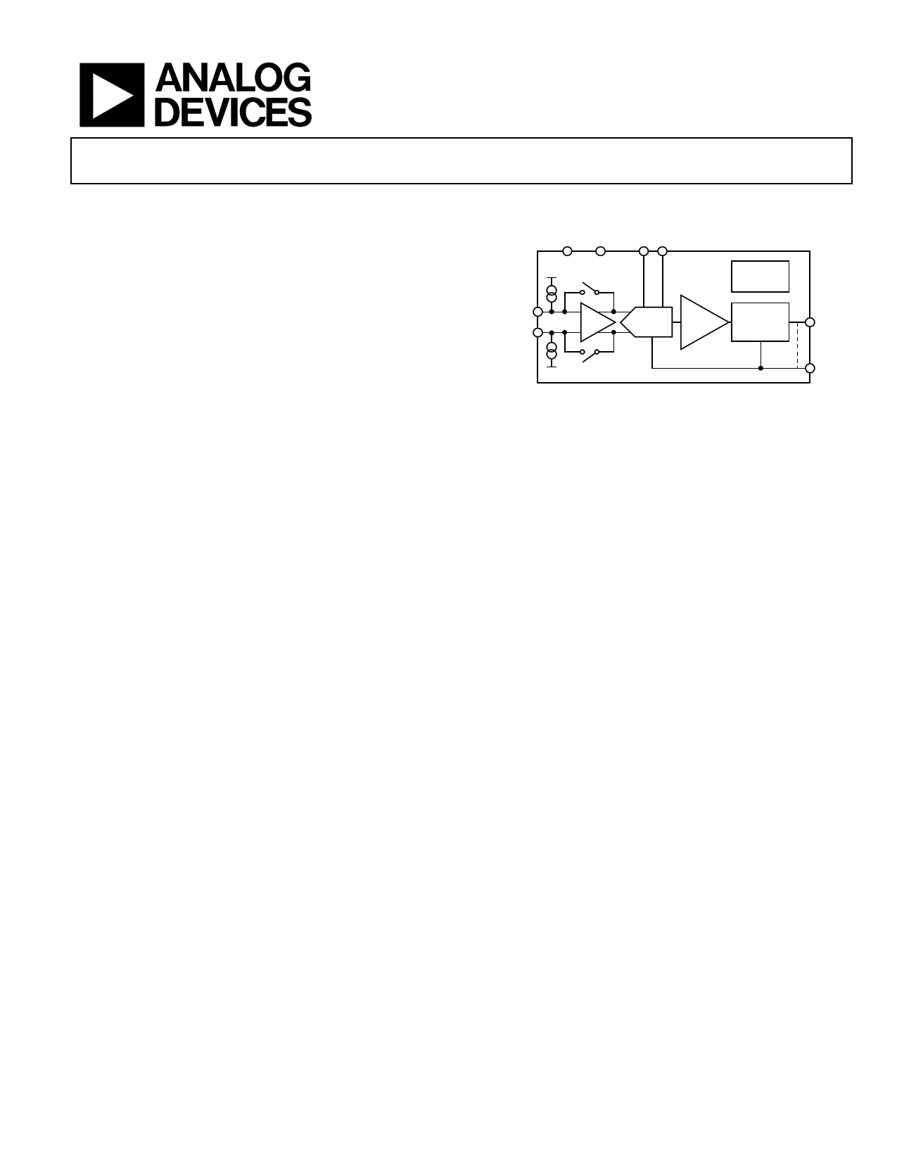
FUNCTIONAL BLOCK DIAGRAM
GND VDD
REFIN
VDD INTERNAL
CLOCK
AIN
BUF
16-BIT
ADC
DIGITAL
PGA
SERIAL
INTERFACE
AD7790
GND
Figure 1.
03538-0-001
GENERAL DESCRIPTION
The AD7790 is a low power, complete analog front end for
low frequency measurement applications. It contains a low
noise 16-bit ∑-Δ ADC with one differential input that can be
buffered or unbuffered along with a digital PGA, which allows
gains of 1, 2, 4, and 8.
The device operates from an internal clock. Therefore, the user
does not have to supply a clock source to the device. The output
data rate from the part is software programmable and can be
varied from 9.5 Hz to 120 Hz, with the rms noise equal to
1.1 μV at the lower update rate. The internal clock frequency
can be divided by a factor of 2, 4, or 8, which leads to a reduc-
tion in the current consumption. The update rate, cutoff
frequency, and settling time will scale with the clock frequency.
The part operates with a power supply from 2.5 V to 5.25 V.
When operating from a 3 V supply, the power dissipation for
the part is 225 μW maximum. It is housed in a 10-lead MSOP.
Rev. A
Document Feedback
Information furnished by Analog Devices is believed to be accurate and reliable. However, no re-
sponsibility is assumed by Analog Devices for its use, nor for any infringements of patents or other
rights of third parties that may result from its use. Specifications subject to change without notice. No
license is granted by implication or otherwise under any patent or patent rights of Analog Devices.
Trademarksandregisteredtrademarksarethepropertyoftheirrespectiveowners.
One Technology Way, P.O. Box 9106, Norwood, MA 02062-9106, U.S.A.
Tel: 781.329.4700 ©2004–2013 Analog Devices, Inc. All rights reserved.
Technical Support
www.analog.com
Free Datasheet http://www.datasheet4u.com/
1 page 
Data Sheet
AD7790
TIMING CHARACTERISTICS1, 2
Table 2. (VDD = 2.5 V to 5.25 V; GND = 0 V, REFIN(+) = 2.5 V, REFIN(–) = GND, CDIV1 = CDIV0 = 0, Input Logic 0 = 0 V,
Input Logic 1 = VDD, unless otherwise noted.)
Parameter
Limit at TMIN, TMAX
(B Version)
Unit
Conditions/Comments
t3
100
ns min
SCLK High Pulsewidth
t4
100
ns min
SCLK Low Pulsewidth
Read Operation
t1 0
ns min
CS Falling Edge to DOUT/RDY Active Time
60
ns max
VDD = 4.75 V to 5.25 V
80
ns max
VDD = 2.5 V to 3.6 V
t23 0
ns min
SCLK Active Edge to Data Valid Delay4
60
ns max
VDD = 4.75 V to 5.25 V
80
ns max
VDD = 2.5 V to 3.6 V
t55, 6
10
ns min
Bus Relinquish Time after CS Inactive Edge
80 ns max
t6
100
ns max
SCLK Inactive Edge to CS Inactive Edge
t7
10
ns min
SCLK Inactive Edge to DOUT/RDY High
Write Operation
t8 0
ns min
CS Falling Edge to SCLK Active Edge Setup Time4
t9
30
ns min
Data Valid to SCLK Edge Setup Time
t10 25
ns min
Data Valid to SCLK Edge Hold Time
t11 0
ns min
CS Rising Edge to SCLK Edge Hold Time
1 Sample tested during initial release to ensure compliance. All input signals are specified with tR = tF = 5 ns (10% to 90% of VDD) and timed from a voltage level of 1.6 V.
2 See Figure 3 and Figure 4.
3 These numbers are measured with the load circuit of Figure 2 and defined as the time required for the output to cross the VOL or VOH limits.
4 SCLK active edge is falling edge of SCLK.
5 These numbers are derived from the measured time taken by the data output to change 0.5 V when loaded with the circuit of Figure 2. The measured number is then
extrapolated back to remove the effects of charging or discharging the 50 pF capacitor. This means that the times quoted in the timing characteristics are the true bus
relinquish times of the part and, as such, are independent of external bus loading capacitances.
6 RDY returns high after a read of the ADC. In single conversion mode and continuous conversion mode, the same data can be read again, if required, while RDY is high,
although care should be taken to ensure that subsequent reads do not occur close to the next output update. In continuous read mode, the digital word can be read
only once.
Rev. A | Page 5 of 20
Free Datasheet http://www.datasheet4u.com/
5 Page 
Data Sheet
AD7790
STATUS REGISTER (RS1, RS0 = 0, 0; POWER-ON/RESET = 0x88)
The status register is an 8-bit read-only register. To access the ADC status register, the user must write to the communications register,
select the next operation to be a read, and load bits RS1 and RS0 with 0. Table 8 outlines the bit designations for the status register. SR0
through SR7 indicate the bit locations, SR denoting the bits are in the status register. SR7 denotes the first bit of the data stream. The
number in brackets indicates the power-on/reset default status of that bit.
SR7 SR6 SR5 SR4 SR3 SR2 SR1 SR0
RDY(1)
ERR(0)
0(0)
0(0)
1(1)
WL(0)
CH1(0)
CH0(0)
Table 8. Status Register Bit Designations
Bit Location Bit Name
Description
SR7 RDY Ready bit for ADC. Cleared when data is written to the ADC data register. The RDY bit is set automatically
after the ADC data register has been read or a period of time before the data register is updated with a
new conversion result to indicate to the user not to read the conversion data. It is also set when the part
is placed in powe-down mode. The end of a conversion is indicated by the DOUT/RDY pin also. This pin
can be used as an alternative to the status register for monitoring the ADC for conversion data.
SR6 ERR ADC Error Bit. This bit is written to at the same time as the RDY bit. Set to indicate that the result written
to the ADC data register has been clamped to all 0s or all 1s. Error sources include overrange, under-
range. Cleared by a write operation to start a conversion.
SR5 0
This bit is automatically cleared.
SR4 0
This bit is automatically cleared.
SR3 1
This bit is automatically set.
SR2 0
This bit is automatically cleared if the device is an AD7790. It can be used to distinguish between the
AD7790 and AD7791, in which the bit is set.
SR1–SR0
CH1–CH0
These bits indicate which channel is being converted by the ADC.
MODE REGISTER (RS1, RS0 = 0, 1; POWER-ON/RESET = 0x02)
The mode register is an 8-bit register from which data can be read or to which data can be written. This register is used to configure the
ADC for range, enable or disable the buffer, or place the device into power-down mode. Table 9 outlines the bit designations for the mode
register. MR0 through MR7 indicate the bit locations, MR denoting the bits are in the mode register. MR7 denotes the first bit of the data
stream. The number in brackets indicates the power-on/reset default status of that bit. Any write to the setup register resets the modulator
and filter and sets the RDY bit.
MR7
MD1(0)
MR6
MD0(0)
MR5
G1(0)
MR4
G0(0)
MR3
BO(0)
MR2
0(0)
MR1
BUF(1)
MR0
0(0)
Table 9. Mode Register Bit Designations
Bit Location Bit Name
Description
MR7–MR6
MD1–MD0
Mode Select Bits. These bits select between continuous conversion mode, single conversion mode, and
standby mode. In continuous conversion mode, the ADC continuously performs conversions and places
the result in the data register. RDY goes low when a conversion is complete. The user can read these
conversions by placing the device in continuous read mode whereby the conversions are automatically
placed on the DOUT line when SCLK pulses are applied. Alternatively, the user can instruct the ADC to
output the conversion by writing to the communications register. After power-on, the first conversion is
available after a period 2/ fADC while subsequent conversions are available at a frequency of fADC. In single
conversion mode, the ADC is placed in power-down mode when conversions are not being performed.
When single conversion mode is selected, the ADC powers up and performs a single conversion, which
occurs after a period 2/fADC. The conversion result in placed in the data register, RDY goes low, and the
ADC returns to power-down mode. The conversion remains in the data register and RDY remains active
(low) until the data is read or another conversion is performed. See Table 10.
MR5–MR4
G1–G0
Range Bits. The AD7790 can be operated with four analog input ranges (see Table 11).
MR3 BO Burnout Current Enable Bit. When this bit is set to 1 by the user, the 100 nA current sources in the signal
path are enabled. When BO = 0, the burnout currents are disabled. The burnout currents can be enabled
only when the buffer is active.
Rev. A | Page 11 of 20
Free Datasheet http://www.datasheet4u.com/
11 Page | ||
| Páginas | Total 20 Páginas | |
| PDF Descargar | [ Datasheet AD7790.PDF ] | |
Hoja de datos destacado
| Número de pieza | Descripción | Fabricantes |
| AD779 | 14-Bit 128 kSPS Complete Sampling ADC | Analog Devices |
| AD7790 | 16-Bit Buffered Sigma-Delta ADC | Analog Devices |
| AD7791 | Buffered 24-Bit Sigma-Delta ADC | Analog Devices |
| AD7792 | (AD7792 / AD7793) 16/24-Bit Sigma-Delta ADC | Analog Devices |
| Número de pieza | Descripción | Fabricantes |
| SLA6805M | High Voltage 3 phase Motor Driver IC. |
Sanken |
| SDC1742 | 12- and 14-Bit Hybrid Synchro / Resolver-to-Digital Converters. |
Analog Devices |
|
DataSheet.es es una pagina web que funciona como un repositorio de manuales o hoja de datos de muchos de los productos más populares, |
| DataSheet.es | 2020 | Privacy Policy | Contacto | Buscar |