|
|
PDF MAX14591 Data sheet ( Hoja de datos )
| Número de pieza | MAX14591 | |
| Descripción | Open-Drain Capable Logic-Level Translator | |
| Fabricantes | Maxim Integrated | |
| Logotipo |  |
|
Hay una vista previa y un enlace de descarga de MAX14591 (archivo pdf) en la parte inferior de esta página. Total 13 Páginas | ||
|
No Preview Available !
EVALUATION KIT AVAILABLE
MAX14591
High-Speed, Open-Drain Capable
Logic-Level Translator
General Description
The MAX14591 is a dual-channel, bidirectional logic-
level translator with the level shifting necessary to allow
data transfer in a multivoltage system. Externally applied
voltages, VCC and VL, set the logic levels on either side
of the device. A logic signal present on the VL side of the
device appears as the same logic signal on the VCC side
of the device, and vice-versa.
The device is optimized for the I2C bus as well as the
management data input/output (MDIO) bus where often
high-speed, open-drain operation is required. When TS
is high, the device allows the pullup to be connected to
the I/O port that has the power. This allows continuous
I2C operation on the powered side without any disruption
while the level translation function is off.
The part is specified over the extended -40NC to +85NC
temperature range, and is available in 8-bump WLP and
8-pin TDFN packages.
Applications
Devices with I2C Communication
Devices with MDIO Communication
General Logic-Level Translation
Benefits and Features
S Meets Industry Standards
I2C Requirements for Standard, Fast, and
High* Speeds
MDIO Open Drain Above 4MHz*
S Allows Greater Design Flexibility
Down to 0.9V Operation on VL Side
Supports Above 8MHz Push-Pull Operation
S Offers Low Power Consumption
23µA (typ) VCC Supply Current
0.5µA (typ) VL Supply Current
S Provides High Level of Integration
Pullup Resistor Enabled with One Side
Power Supply when TS Is High
12kI (max) Internal Pullup
Low Transmission Gate RON: 17I (max)
S Saves Space
8-Bump, 0.4mm pitch, 0.8mm x 1.6mm WLP
Package
8-Pin, 2mm x 2mm TDFN Package
*Requires external pullups.
Ordering Information appears at end of data sheet.
VL = +1.2V
+1.2V
SYSTEM
CONTROLLER
EN
SDA
Typical Operating Circuit
0.1µF
1µF
VCC = +3.0V
TS VL
VCC
VL
* MAX14591
VCC
*
+3V
SYSTEM
IOVL1
VL
*
IOVCC1
SDA
VCC
*
GND SLK
IOVL2
GND IOVCC2
SLK GND
* PULLUPS ARE OPTIONAL FOR HIGH-SPEED, OPEN-DRAIN OPERATION.
For pricing, delivery, and ordering information, please contact Maxim Direct at
1-888-629-4642, or visit Maxim Integrated’s website at www.maximintegrated.com.
19-6173; Rev 1; 12/14
1 page 
MAX14591
High-Speed, Open-Drain Capable
Logic-Level Translator
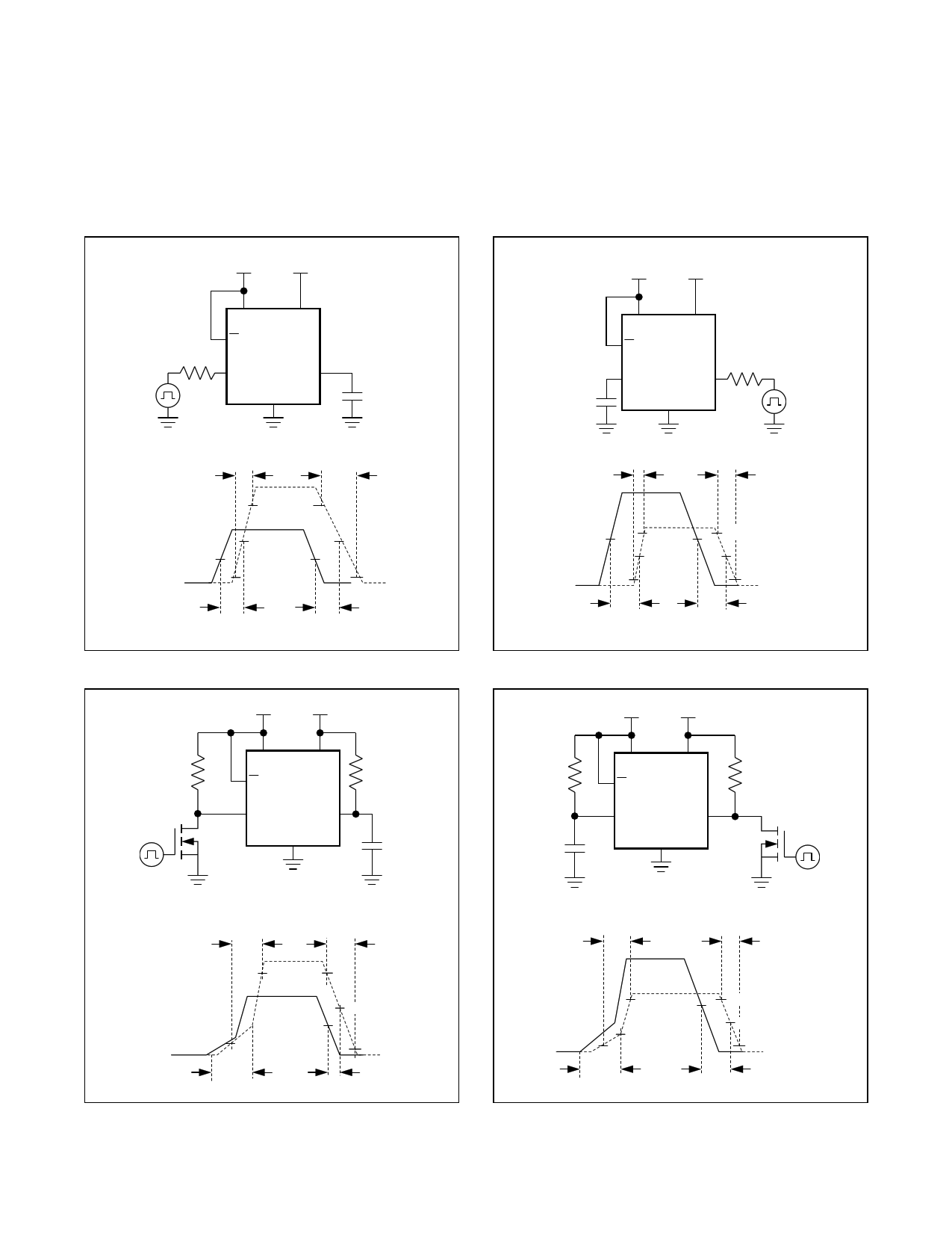
VL VCC
VL VCC
RS TS MAX14591
50I
IOVL_
IOVCC_
GND
CL
20pF
VL VCC
VL VCC
TS MAX14591
IOVL_
IOVCC_
RS
50I
CL
20pF
GND
tRCC tFCC
90% 90%
50% 50%
50% 50%
10% 10%
tPD_LCC
tPD_LCC
Figure 1. Push-Pull Driving IOVL_
VL VCC
VL VCC
1kI TS MAX14591
RDSON
5I
IOVL_
IOVCC_
GND
1kI
CL
20pF
tRL tFL
50%
90% 50%
90%
50% 50%
10% 10%
tPD_CCL
tPD_CCL
Figure 3. Push-Pull Driving IOVCC_
VL VCC
1kI
CL
20pF
VL VCC
TS MAX14591
IOVL_
IOVCC_
GND
1kI
RDSON
5I
tRCC tFCC
90% 90%
50%
50%
10% 10%
tPD_LCC
Figure 2. Open-Drain Driving IOVL_
tPD_LCC
Maxim Integrated
tRL tFL
90%
10%
tPD_CCL
50% 90%
50%
10%
tPD_CCL
Figure 4. Open-Drain Driving IOVCC_
5
5 Page 
MAX14591
High-Speed, Open-Drain Capable
Logic-Level Translator
Applications Information
Layout Recommendations
Use standard high-speed layout practices when
laying out a board with the MAX14591. For example, to
minimize line coupling, place all other signal lines not con-
nected to the device at least 1x the substrate height of the
PCB away from the input and output lines of the device.
Extended ESD
ESD protection structures are incorporated on all pins to
protect against electrostatic discharges up to ±2kV (HBM)
encountered during handling and assembly. After an ESD
event, the device continues to function without latchup.
ESD Test Conditions
ESD performance depends on a variety of conditions.
Contact Maxim for a reliability report that documents test
setup, test methodology, and test results.
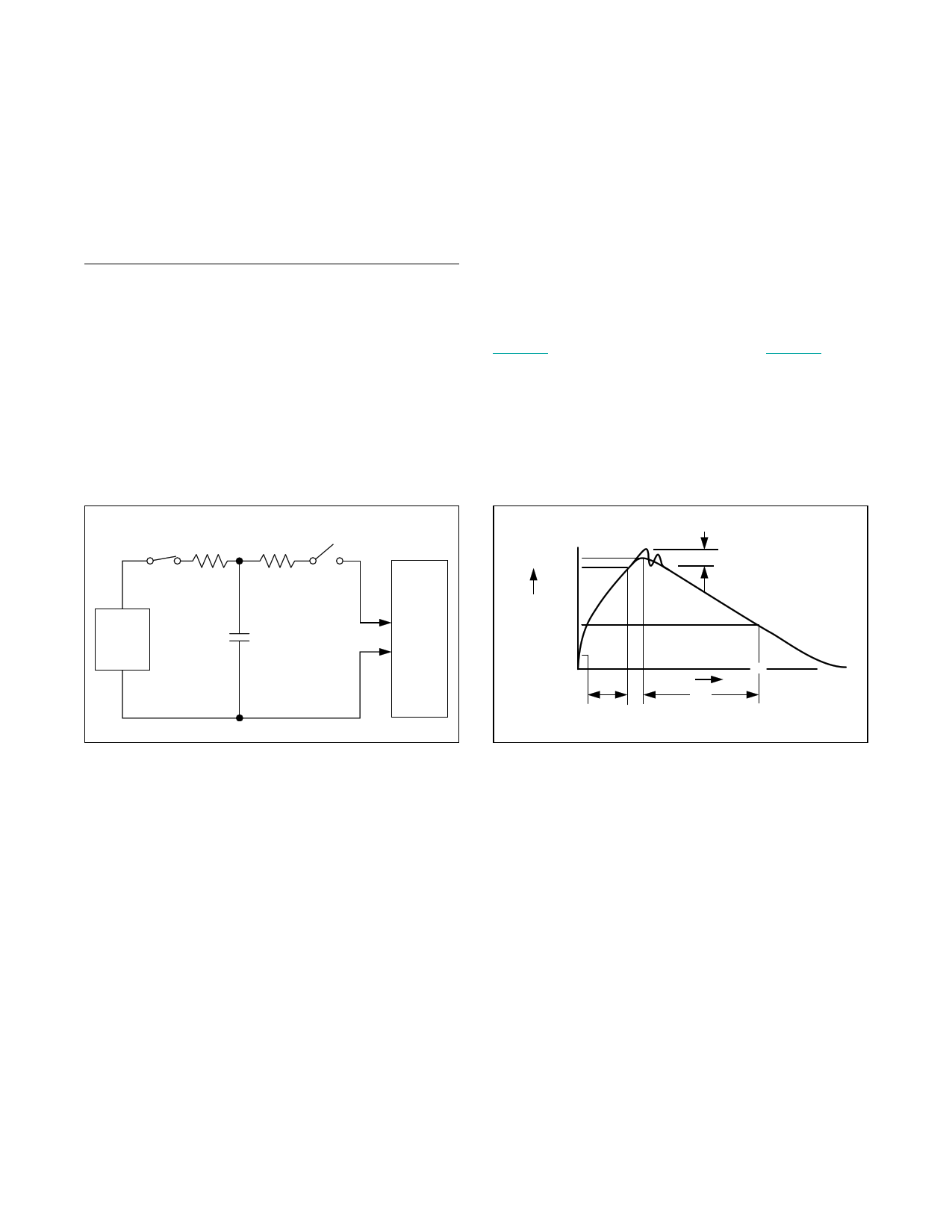
Human Body Model
Figure 5 shows the Human Body Model. Figure 6 shows
the current waveform it generates when discharged
into a low impedance. This model consists of a 100pF
capacitor charged to the ESD voltage of interest that is
then discharged into the device through a 1.5kI resistor.
RC
1MI
CHARGE CURRENT-
LIMIT RESISTOR
HIGH-
VOLTAGE
DC
SOURCE
CS
100pF
RD
1.5kI
DISCHARGE
RESISTANCE
STORAGE
CAPACITOR
Figure 5. Human Body ESD Test Model
DEVICE
UNDER
TEST
IP 100%
90%
AMPERES
36.8%
10%
0
0
tRL
Ir PEAK-TO-PEAK RINGING
(NOT DRAWN TO SCALE)
TIME
tDL
CURRENT WAVEFORM
Figure 6. Human Body Current Waveform
Maxim Integrated
11
11 Page | ||
| Páginas | Total 13 Páginas | |
| PDF Descargar | [ Datasheet MAX14591.PDF ] | |
Hoja de datos destacado
| Número de pieza | Descripción | Fabricantes |
| MAX1459 | 2-Wire / 4-20mA Smart Signal Conditioner | Maxim Integrated |
| MAX14590 | (MAX14586 / MAX14590) High-Current Overvoltage Protectors | Maxim Integrated |
| MAX14591 | Open-Drain Capable Logic-Level Translator | Maxim Integrated |
| MAX14595 | Low-Power Dual-Channel Logic-Level Translator | Maxim Integrated |
| Número de pieza | Descripción | Fabricantes |
| SLA6805M | High Voltage 3 phase Motor Driver IC. |
Sanken |
| SDC1742 | 12- and 14-Bit Hybrid Synchro / Resolver-to-Digital Converters. |
Analog Devices |
|
DataSheet.es es una pagina web que funciona como un repositorio de manuales o hoja de datos de muchos de los productos más populares, |
| DataSheet.es | 2020 | Privacy Policy | Contacto | Buscar |
