|
|
|
PDF X45620 Data sheet ( Hoja de datos )
| Número de pieza | X45620 | |
| Descripción | Dual Voltage Monitor | |
| Fabricantes | Intersil | |
| Logotipo | ||
Hay una vista previa y un enlace de descarga de X45620 (archivo pdf) en la parte inferior de esta página. Total 20 Páginas | ||
|
No Preview Available !
®
Data Sheet
July 29, 2005
X45620
FN8250.0
Dual Voltage Monitor with Integrated
System Battery Switch and EEPROM
FEATURES
• Dual voltage monitoring
• Active low reset outputs
• Two standard reset threshold voltages
—Factory programmable threshold
• Lowline Output — zero delayed POR
• Reset signal valid to VCC = 1V
• System battery switch-over circuitry
• Selectable watchdog timer
—(0.15s, 0.4s, 0.8s, off)
• 256Kbits of EEPROM
• Built-in inadvertent write protection
—Power-up/power-down protection circuitry
—Protect 0, 1/4, 1/2 or all of EEPROM array with
programmable Block Lock™ protection
—In circuit programmable ROM mode
• Minimize EEPROM programming time
—64 byte page write mode
—Self-timed write cycle
—5ms write cycle time (typical)
• 400kHz 2-wire Interface
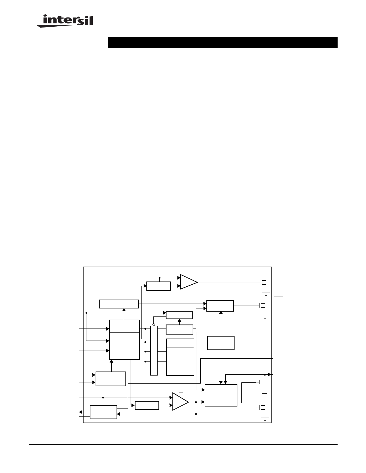
BLOCK DIAGRAM
• 2.7V to 5.5V power supply operation
• Available package — 20-lead TSSOP
• Dual supervisor
• Battery switch and output
DESCRIPTION
The Intersil X45620 combines power-on reset control,
battery switch circuit, watchdog timer, supply voltage
supervision, secondary voltage supervision, block lock
protect and serial EEPROM in one package. This
combination lowers system cost, reduces board space
requirements, and increases reliability.
Applying power to the device activates the power-on
reset circuit which holds RESET active for a period of
time. This allows the power supply and oscillator to
stabilize before the processor can execute code.
A system battery switch circuit compares VCC (V1MON)
with VBATT input and connects VOUT to whichever is
higher. This provides voltage to external SRAM or other
circuits in the event of main power failure. The X45620
can drive 50mA from VCC and 250µA from VBATT. The
device switches to VBATT when VCC drops below the
low VCC voltage threshold and VBATT > VCC.
V2MON
WP
SDA
SCL
S0
S1
VCC
(V1MON)
VOUT
VBATT
V2 Monitor
Logic
VOUT
+
VTRIP2
-
Watchdog Transition
Detector
Data
Register
Command
Decode, Test
& Control
Logic
Device
Select
Logic
System
Battery
Switch
VCC Monitor
Logic
Protect Logic
Status
Register
EEPROM
Array
512 X 512
(32K X 8 Bit)
VOUT
+
VTRIP1
-
Watchdog
Timer Reset
Reset &
Watchdog
Timebase
Power-on,
Low Voltage
Reset
Generation
V2FAIL
WDO
BATT-ON
RESET/MR
LOWLINE
1
CAUTION: These devices are sensitive to electrostatic discharge; follow proper IC Handling Procedures.
1-888-INTERSIL or 1-888-468-3774 | Intersil (and design) is a registered trademark of Intersil Americas Inc.
Copyright Intersil Americas Inc. 2005. All Rights Reserved
All other trademarks mentioned are the property of their respective owners.
Free Datasheet http://www.datasheet4u.com/
1 page 
X45620
D.C. OPERATING CHARACTERISTICS (CONTINUED)
(Over recommended operating conditions unless otherwise specified)
Symbol
VOLR
Parameter
Output (RESET, LOWLINE, WDO,
V2FAIL) LOW Voltage
Two Wire Interface
VIL
VIH
ILI
VOLS
Input (SDA, S0, S1, SCL, WP) LOW
Voltage
Input (SDA, S0, S1, SCL, WP) HIGH
Voltage
Input Leakage Current (SDA, S1, S0,
SCL, WP)
Output (SDA) LOW Voltage
Limits
Min Typ (6) Max Unit Test Conditions
0.4 V IOL = 3.0mA (5V)
IOL = 1.0mA (3V)
-0.5
VCC x 0.7
VCC x 0.3 V Note 3
VCC + 0.5 V Note 3
±10 µA
0.4 V IOL = 3.0mA (5V)
IOL = 1.0mA (3V), Note 4
Notes: (1) The device enters the Active state after any start, and remains active until 9 clock cycles later if the Device Select Bits in the Slave
Address Byte are incorrect; 200ns after a stop ending a read operation; or tWC after a stop ending a write operation.
(2) The device goes into Standby: 200ns after any Stop, except those that initiate a high voltage write cycle; tWC after a stop that initiates a
high voltage cycle; or 9 clock cycles after any start that is not followed by the correct Device Select Bits in the Slave Address Byte.
(3) VIL min. and VIH max. are for reference only and are not tested.
(4) This parameter is guaranteed by characterization.
CAPACITANCE TA = +25°C, f = 1MHz, VCC = 5V
Symbol
Test
COUT Output Capacitance (SDA, RESET, V2FAIL, LOWLINE, BATT-ON, WDO)
CIN Input Capacitance (SDA, SCL, S0, S1, WP)
Max
8
6
Unit
pF
pF
Conditions
VOUT = 0V,
Note 1, 4
VIN = 0V,
Note 1, 4
EQUIVALENT A.C. LOAD CIRCUIT AT 5V VCC
VCC
VCC
1.53kΩ
1.53kΩ
A.C. TEST CONDITIONS
Input pulse levels
Input rise and fall times
Input and output timing level
VCC x 0.1 to VCC x 0.9
10ns
VCC x 0.5
SDA
RESET
V2FAIL
LOWLINE
WDO
BATT-ON
30pF
30pF 4481Ω
5 FN8250.0
July 29, 2005
Free Datasheet http://www.datasheet4u.com/
5 Page 
X45620
System Battery Switch
As long as VCC exceeds the low voltage detect thresh-
old VTRIP1, VOUT is connected to VCC through a 5Ω
(typical) switch. When the VCC has fallen below VTRIP,
then VCC is applied to VOUT if VCC is equal to or
greater than VBATT + 0.03V. When VCC drops to less
than VBATT - 0.03V, then VOUT is connected to VBATT
through an 80Ω (typical) switch. VOUT typically sup-
plies the system static RAM voltage, so the switchover
circuit operates to protect the contents of the static
RAM during a power failure. Typically, when VCC has
failed, the SRAMs go into a lower power state and
draw much less current than in their active mode.
When VCC returns, VOUT switches back to VCC when
VCC exceeds VBATT+0.03V. There is a 60mV hystere-
sis around this battery switch threshold to prevent
oscillations between supplies.
While VCC is connected to VOUT the BATT-ON pin is
pulled LOW. The signal can drive external pass ele-
ments to provide additional current to the external cir-
cuits during normal operation.
Operation
The device is in normal operation with VCC as long as
VCC > VTRIP1. It switches to the battery backup mode
when VCC goes away.
Condition
VCC > VTRIP1
VCC > VTRIP1 &
VBATT = 0
0 ≤ VCC < VTRIP1
and VCC < VBATT
Mode of Operation
Normal Operation.
Normal Operation without battery
back up capability.
Battery Backup Mode; RESET
signal is asserted. No communica-
tion to the device is allowed.
Manual Reset
By connecting a push-button from MR to ground or
driven by logic, the designer adds manual system reset
capability. The RESET pins is asserted when the push-
button is closed and remain asserted for tPURST after the
push-button is released. This pin is debounced so a
push-button connected directly to the device will have
both clean falling and rising edges on MR.
Figure 2. Example System Connection
Unregulated
Supply
5V
Reg
Dual P-channel FET
Examples: IRF 7756, FDS9733A
V2MON
Provides
Early Detection
of Power Failure
+
Supercap
VCC BATT-ON
VOUT
VBATT
V2MON
V2FAIL
RESET
SDA, SCL
VSS
SRAM
Address
Decode
Enable
NMI
Addr
VCC
RESET
2-Wire µC
11 FN8250.0
July 29, 2005
Free Datasheet http://www.datasheet4u.com/
11 Page | ||
| Páginas | Total 20 Páginas | |
| PDF Descargar | [ Datasheet X45620.PDF ] | |
Hoja de datos destacado
| Número de pieza | Descripción | Fabricantes |
| X45620 | Dual Voltage Monitor | Intersil |
| Número de pieza | Descripción | Fabricantes |
| SLA6805M | High Voltage 3 phase Motor Driver IC. |
Sanken |
| SDC1742 | 12- and 14-Bit Hybrid Synchro / Resolver-to-Digital Converters. |
Analog Devices |
|
DataSheet.es es una pagina web que funciona como un repositorio de manuales o hoja de datos de muchos de los productos más populares, |
| DataSheet.es | 2020 | Privacy Policy | Contacto | Buscar |