|
|
|
PDF NCP1216A Data sheet ( Hoja de datos )
| Número de pieza | NCP1216A | |
| Descripción | PWM Current-Mode Controller | |
| Fabricantes | ON Semiconductor | |
| Logotipo | ||
Hay una vista previa y un enlace de descarga de NCP1216A (archivo pdf) en la parte inferior de esta página. Total 18 Páginas | ||
|
No Preview Available !
NCP1216, NCP1216A
PWM Current-Mode
Controller for High-Power
Universal Off-Line Supplies
Housed in a SOIC−8 or PDIP−7 package, the NCP1216 represents
an enhanced version of NCP1200 based controllers. Due to its high
drive capability, NCP1216 drives large gate−charge MOSFETs, which
together with internal ramp compensation and built−in frequency
jittering, ease the design of modern AC−DC adapters.
With an internal structure operating at different fixed frequencies,
the controller supplies itself from the high−voltage rail, avoiding the
need of an auxiliary winding. This feature naturally eases the designer
task in some particular applications, e.g. battery chargers or TV sets.
Current−mode control also provides an excellent input audio
susceptibility and inherent pulse−by−pulse control. Internal ramp
compensation easily prevents sub−harmonic oscillations from taking
place in continuous conduction mode designs.
When the current setpoint falls below a given value, e.g. the output
power demand diminishes, the IC automatically enters the so−called
skip cycle mode and provides excellent efficiency at light loads.
Because this occurs at a user adjustable low peak current, no acoustic
noise takes place.
The NCP1216 features an efficient protective circuitry, which in
presence of an over current condition disables the output pulses while
the device enters a safe burst mode, trying to restart. Once the default
has gone, the device auto−recovers.
Features
• No Auxiliary Winding Operation
• Current−Mode Control with Adjustable Skip−Cycle Capability
• Internal Ramp Compensation
• Limited Duty Cycle to 50% (NCP1216A Only)
• Internal 1.0 ms Soft−Start (NCP1216A Only)
• Built−In Frequency Jittering for Better EMI Signature
• Auto−Recovery Internal Output Short−Circuit Protection
• Extremely Low No−Load Standby Power
• 500 mA Peak Current Capability
• Fixed Frequency Versions at 65 kHz, 100 kHz, 133 kHz
• Internal Temperature Shutdown
• Direct Optocoupler Connection
• SPICE Models Available for TRANsient and AC Analysis
• Pin−to−Pin Compatible with NCP1200 Series
• These are Pb−Free and Halide−Free Devices
Typical Applications
• High Power AC−DC Converters for TVs, Set−Top Boxes, etc.
• Offline Adapters for Notebooks
• Telecom DC−DC Converters
• All Power Supplies
www.onsemi.com
8
1
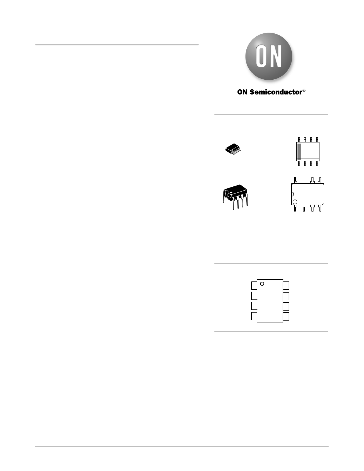
SOIC−8
D SUFFIX
CASE 751
MARKING
DIAGRAMS
8
XXXXX
ALYW
G
1
PDIP−7
P SUFFIX
CASE 626B
XXXXXXXXX
AWL
YYWWG
1
XXXXXX = Specific Device Code
A = Assembly Location
WL, L = Wafer Lot
YY, Y = Year
WW, W = Work Week
G or G = Pb−Free Package
PIN CONNECTIONS
Adj 1
FB 2
CS 3
Gnd 4
8 HV
7 NC
6 VCC
5 Drv
DEVICE MARKING AND
ORDERING INFORMATION
See detailed ordering and shipping information in the ordering
information section on page 16 of this data sheet.
© Semiconductor Components Industries, LLC, 2016
May, 2016 − Rev. 16
1
Publication Order Number:
NCP1216/D
1 page 
NCP1216, NCP1216A
ELECTRICAL CHARACTERISTICS (continued)
(For typical values TJ = 25°C, for min/max values TJ = −40°C to +125°C, Maximum TJ = 150°C, VCC = 11 V unless otherwise noted.)
Characteristic
Pin Symbol Min Typ Max Unit
INTERNAL OSCILLATOR (VCC = 11 V, Pin 5 Loaded by 1.0 kW)
Oscillation Frequency, 65 kHz Version
0°C ≤ TJ ≤ +125°C
−40°C ≤ TJ ≤ +125°C
Oscillation Frequency, 100 kHz Version
0°C ≤ TJ ≤ +125°C
−40°C ≤ TJ ≤ +125°C
Oscillation Frequency, 133 kHz Version
0°C ≤ TJ ≤ +125°C
−40°C ≤ TJ ≤ +125°C
Built−in Frequency Jittering in Percentage of fOSC
Maximum Duty−Cycle
NCP1216
NCP1216A
fOSC
fOSC
fOSC
fjitter
Dmax
kHz
58.5 65 71.5
57 65 75
kHz
90 100 110
86 100 120
kHz
120 133 146
110 133 160
±4.0 %
69 75 81 %
42 46.5 50
FEEDBACK SECTION (VCC = 11 V, Pin 5 Loaded by 1.0 kW)
Internal Pullup Resistor
Pin 2 (FB) to Internal Current Setpoint Division Ratio
SKIP CYCLE GENERATION
2 Rup
− Iratio
20 kW
3.3
Default Skip Mode Level
Pin 1 Internal Output Impedance
INTERNAL RAMP COMPENSATION
1 Vskip 0.9 1.1 1.26 V
1 Zout
25 kW
Internal Ramp Level @ 25°C (Note 3)
3 Vramp
2.6
2.9
3.2 V
Internal Ramp Resistance to CS Pin
3 Rramp
19 kW
Product parametric performance is indicated in the Electrical Characteristics for the listed test conditions, unless otherwise noted. Product
performance may not be indicated by the Electrical Characteristics if operated under different conditions.
3. A 1.0 MW resistor is connected to the ground for the measurement.
www.onsemi.com
5
5 Page 
NCP1216, NCP1216A
the nominal switching frequency whose sweep is
synchronized with the VCC ripple. For instance, with a 2.2 V
peak−to−peak ripple, the NCP1216P065 frequency will
equal 65 kHz in the middle of the ripple and will increase as
VCC rises or decrease as VCC ramps down. Figure 20
portrays the behavior we have adopted:
To better understand how this skip cycle mode takes place,
a look at the operation mode versus the FB level
immediately gives the necessary insight:
FB
VCCOFF
VCC Ripple
68 kHz
4.2 V, FB Pin Open
65 kHz
62 kHz
VCCON
Figure 20. VCC Ripple is Used to Introduce a
Frequency Jittering on the Internal Oscillator
Sawtooth
Skipping Cycle Mode
The NCP1216 automatically skips switching cycles when
the output power demand drops below a given level. This is
accomplished by monitoring the FB pin. In normal
operation, pin 2 imposes a peak current accordingly to the
load value. If the load demand decreases, the internal loop
asks for less peak current. When this setpoint reaches a
determined level, the IC prevents the current from
decreasing further down and starts to blank the output
pulses: the IC enters the so−called skip cycle mode, also
named controlled burst operation. The power transfer now
depends upon the width of the pulse bunches (Figure 22).
Suppose we have the following component values:
Lp, primary inductance = 350 mH
Fsw, switching frequency = 65 kHz
Ip skip = 600 mA (or 333 mV / Rsense)
The theoretical power transfer is therefore:
1
2
Lp
Ip2
Fsw + 4 W.
(eq. 8)
If this IC enters skip cycle mode with a bunch length of
10 ms over a recurrent period of 100 ms, then the total power
transfer is:
4 0.1 + 400 mW.
(eq. 9)
Normal Current Mode Operation
Skip Cycle Operation
IpMIN = 333 mV / Rsense
3.2 V, Upper
Dynamic Range
1V
Figure 21.
When FB is above the skip cycle threshold (1.0 V by
default), the peak current cannot exceed 1.0 V/Rsense. When
the IC enters the skip cycle mode, the peak current cannot go
below Vpin1 / 3.3. The user still has the flexibility to alter this
1.0 V by either shunting pin 1 to ground through a resistor
or raising it through a resistor up to the desired level.
Grounding pin 1 permanently invalidates the skip cycle
operation.
Power P1
Power
P2
Power
P3
Figure 22. Output Pulses at Various Power Levels
(X = 5 ms/div) P1 < P2 < P3
www.onsemi.com
11
11 Page | ||
| Páginas | Total 18 Páginas | |
| PDF Descargar | [ Datasheet NCP1216A.PDF ] | |
Hoja de datos destacado
| Número de pieza | Descripción | Fabricantes |
| NCP1216 | PWM Current-Mode Controller | ON |
| NCP1216A | PWM Current-Mode Controller | ON Semiconductor |
| Número de pieza | Descripción | Fabricantes |
| SLA6805M | High Voltage 3 phase Motor Driver IC. |
Sanken |
| SDC1742 | 12- and 14-Bit Hybrid Synchro / Resolver-to-Digital Converters. |
Analog Devices |
|
DataSheet.es es una pagina web que funciona como un repositorio de manuales o hoja de datos de muchos de los productos más populares, |
| DataSheet.es | 2020 | Privacy Policy | Contacto | Buscar |