|
|
|
PDF ADP170 Data sheet ( Hoja de datos )
| Número de pieza | ADP170 | |
| Descripción | (ADP170 / ADP171) CMOS Linear Regulators | |
| Fabricantes | Analog Devices | |
| Logotipo | ||
Hay una vista previa y un enlace de descarga de ADP170 (archivo pdf) en la parte inferior de esta página. Total 20 Páginas | ||
|
No Preview Available !
300 mA, Low Quiescent Current,
CMOS Linear Regulators
ADP170/ADP171
FEATURES
Maximum output current: 300 mA
Input voltage range: 1.6 V to 3.6 V
Low quiescent current
IGND = 23 μA with 0 mA load
IGND = 170 μA with 300 mA load
Low shutdown current: <1 μA
Low dropout voltage: 66 mV at 300 mA load
Output voltage accuracy: ±1%
Up to 31 fixed-output voltage options available from 0.8 V to
3.0 V
Adjustable-output voltage range
0.8 V to 3.0 V (ADP171)
Accuracy over line, load, and temperature: ±3%
Stable with small 1 μF ceramic output capacitor
PSRR performance of 70 dB at 10 kHz and 73 dB at 1 kHz
Low noise: 30 μV rms at VOUT = 0.8 V
Current limit and thermal overload protection
Logic-controlled enable
Compact 5-lead TSOT package
APPLICATIONS
Mobile phones
Digital camera and audio devices
Portable and battery-powered equipment
DSP/FPGA/microprocessor supplies
Post dc-dc regulation
GENERAL DESCRIPTION
The ADP170/ADP171 are low voltage input, low quiescent
current, low-dropout (LDO) linear regulators that operate from
1.6 V to 3.6 V and provide up to 300 mA of output current. The
low 66 mV dropout voltage at 300 mA load improves efficiency
and allows operation over a wide input voltage range. The low
23 μA of quiescent current at a 0 mA load makes the ADP170/
ADP171 ideal for battery-operated portable equipment.
The ADP170 is capable of 31 fixed-output voltage options, ranging
from 0.8 V to 3.0 V. ADP171 is an adjustable version, which allows
output voltages that range from 0.8 V to 3.0 V via an external
divider. The ADP170/ADP171 are optimized for stable operation
with small 1 μF ceramic output capacitors. Ideal for powering
digital processors, the ADP170/ADP171 exhibit good transient
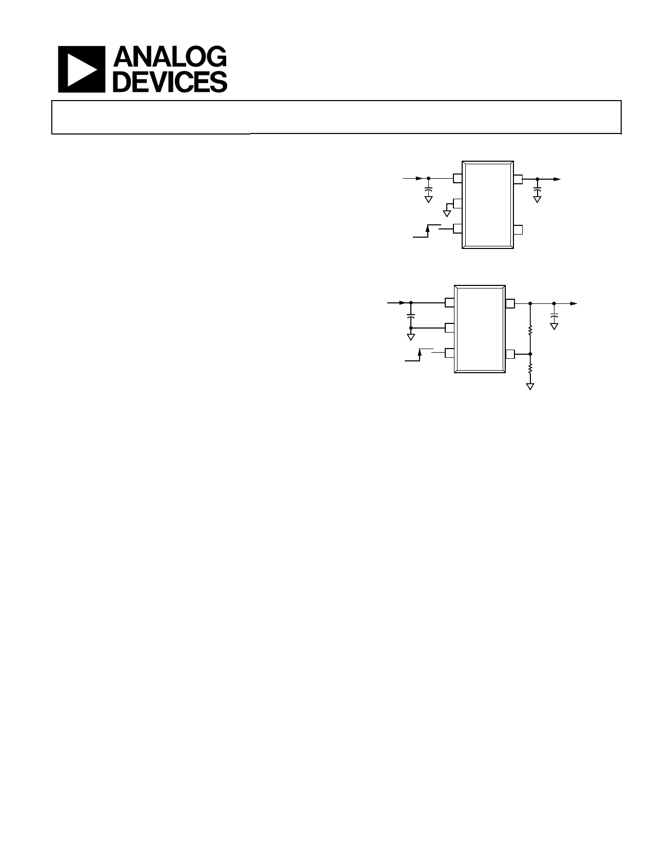
TYPICAL APPLICATION CIRCUITS
VIN
C1
ON
OFF
1 VIN VOUT 5
ADP170
C2
2 GND
VOUT
3 EN
NC 4
Figure 1. ADP170 with Fixed Output Voltage, 1.8 V
VIN = 2.3V
CIN
1µF
ON
OFF
1 VIN VOUT 5
ADP171
2 GND
3 EN
ADJ 4
VOUT = 1.8V
COUT
1µF
R1
R2
Figure 2. ADP171 with Adjustable Output Voltage
performance and occupy minimal board space. Compared with
commodity types of LDOs, the ADP170/ADP171 provide 20 dB
to 40 dB better power supply rejection ratio (PSRR) at 100 kHz,
making the ADP170/ADP171 an ideal power source for analog-
to-digital converter (ADC) mixed-signal processor systems and
allowing use of smaller size bypass capacitors. In addition, low
output noise performance without the need for an additional
bypass capacitor further reduces printed circuit board (PCB)
component count.
Short-circuit protection and thermal overload protection circuits
prevent damage in adverse conditions. The ADP170/ADP171
are available in tiny 5-lead TSOT for the smallest footprint
solution to meet a variety of portable power applications.
Rev. B
Information furnished by Analog Devices is believed to be accurate and reliable. However, no
responsibility is assumed by Analog Devices for its use, nor for any infringements of patents or other
rights of third parties that may result from its use. Specifications subject to change without notice. No
license is granted by implication or otherwise under any patent or patent rights of Analog Devices.
Trademarksandregisteredtrademarksarethepropertyoftheirrespectiveowners.
One Technology Way, P.O. Box 9106, Norwood, MA 02062-9106, U.S.A.
Tel: 781.329.4700
www.analog.com
Fax: 781.461.3113 ©2009–2010 Analog Devices, Inc. All rights reserved.
Free Datasheet http://www.datasheet4u.com/
1 page 
ABSOLUTE MAXIMUM RATINGS
Table 3.
Parameter
VIN to GND
VOUT to GND
EN to GND
Storage Temperature Range
Operating Junction Temperature Range
Operating Ambient Temperature Range
Soldering Conditions
Rating
−0.3 V to +3.6 V
−0.3 V to VIN
−0.3 V to +3.6 V
−65°C to +150°C
−40°C to +125°C
−40°C to +85°C
JEDEC J-STD-020
Stresses above those listed under absolute maximum ratings
may cause permanent damage to the device. This is a stress
rating only and functional operation of the device at these or
any other conditions above those indicated in the operational
section of this specification is not implied. Exposure to absolute
maximum rating conditions for extended periods may affect
device reliability.
THERMAL DATA
Absolute maximum ratings apply only individually, not in
combination. The ADP170/ADP171 can be damaged when the
junction temperature limits are exceeded. Monitoring ambient
temperature does not guarantee that TJ is within the specified
temperature limits. In applications with high power dissipation
and poor thermal resistance, the maximum ambient temperature
may have to be derated.
In applications with moderate power dissipation and low PCB
thermal resistance, the maximum ambient temperature can
exceed the maximum limit as long as the junction temperature
is within specification limits. The junction temperature (TJ) of
the device is dependent on the ambient temperature (TA), the
power dissipation of the device (PD), and the junction-to-
ambient thermal resistance of the package (θJA).
Maximum junction temperature (TJ) is calculated from the
ambient temperature (TA) and power dissipation (PD) using the
following formula:
TJ = TA + (PD × θJA)
Junction-to-ambient thermal resistance (θJA) of the package is
based on modeling and calculation using a 4-layer board. The
junction-to-ambient thermal resistance is highly dependent on
the application and board layout. In applications where high
ADP170/ADP171
maximum power dissipation exists, close attention to thermal
board design is required. The value of θJA may vary, depending
on PCB material, layout, and environmental conditions. The
specified values of θJA are based on a 4-layer, 4 in. × 3 in. PCB.
Refer to JESD 51-7 for detailed information regarding board
construction.
ΨJB is the junction-to-board thermal characterization parameter
with units of °C/W. The ΨJB of the package is based on modeling
and calculation using a 4-layer board. The Guidelines for Reporting
and Using Electronic Package Thermal Information: JESD51-12
states that thermal characterization parameters are not the same
as thermal resistances. ΨJB measures the component power flowing
through multiple thermal paths rather than a single path as in
thermal resistance, θJB. Therefore, ΨJB thermal paths include
convection from the top of the package as well as radiation from
the package—factors that make ΨJB more useful in real-world
applications. Maximum junction temperature (TJ) is calculated
from the board temperature (TB) and power dissipation (PD)
using the formula
TJ = TB + (PD × ΨJB)
Refer to JESD51-8 and JESD51-12 for more detailed information
about ΨJB.
THERMAL RESISTANCE
θJA and ΨJB are specified for the worst-case conditions, that is, a
device soldered in a circuit board for surface-mount packages.
Table 4. Thermal Resistance
Package Type
θJA
5-Lead TSOT
170
ΨJB
43
Unit
°C/W
ESD CAUTION
Rev. B | Page 5 of 20
Free Datasheet http://www.datasheet4u.com/
5 Page 
THEORY OF OPERATION
The ADP170/ADP171 are low quiescent current, low-dropout
linear regulators that operate from 1.6 V to 3.6 V and can provide
up to 300 mA of output current. Drawing a low 170 μA of quies-
cent current (typical) at full load makes the ADP170/ADP171
ideal for battery-operated portable equipment. Shutdown current
consumption is typically 100 nA.
Optimized for use with small 1 μF ceramic capacitors, the
ADP170/ADP171 provide excellent transient performance.
ADP170
VIN VOUT
GND
SHORT CIRCUIT,
UVLO AND
THERMAL
PROTECT
R1
EN SHUTDOWN
0.5V REFERENCE
R2
NOTES
1. R1 AND R2 ARE INTERNAL RESISTORS, AVAILABLE ON
THE ADP170 ONLY.
Figure 25. ADP170 Internal Block Diagram
ADP171
VIN
VOUT
GND
SHORT CIRCUIT,
UVLO AND
THERMAL
PROTECT
EN SHUTDOWN
0.5V REFERENCE
ADJ
Figure 26. ADP171 Internal Block Diagram
ADP170/ADP171
Internally, the ADP170/ADP171 consist of a reference, an error
amplifier, a feedback voltage divider, and a PMOS pass transistor.
Output current is delivered via the PMOS pass device, which is
controlled by the error amplifier. The error amplifier compares
the reference voltage with the feedback voltage from the output
and amplifies the difference. If the feedback voltage is lower than
the reference voltage, the gate of the PMOS device is pulled lower,
allowing more current to pass and increasing the output voltage.
If the feedback voltage is higher than the reference voltage, the
gate of the PMOS device is pulled higher, allowing less current
to pass and decreasing the output voltage.
The adjustable ADP171 has an output voltage range of 0.8 V to
3.0 V. The output voltage is set by the ratio of two external resistors,
as shown in Figure 2. The device servos the output to maintain
the voltage at the ADJ pin at 0.5 V referenced to ground. The
current in R1 is then equal to 0.5 V/R2 and the current in R1 is
the current in R2 plus the ADJ pin bias current. The ADJ pin
bias current, 15 nA at 25°C, flows through R1 into the ADJ pin.
The output voltage can be calculated using the equation:
VOUT = 0.5 V(1 + R1/R2) + (ADJI-BIAS)(R1)
The value of R1 should be less than 200 kΩ to minimize errors
in the output voltage caused by the ADJ pin bias current. For
example, when R1 and R2 each equal 200 kΩ, the output voltage
is 1.0 V. The output voltage error introduced by the ADJ pin
bias current is 3 mV or 0.3%, assuming a typical ADJ pin bias
current of 15 nA at 25°C.
Note that in shutdown, the output is turned off and the divider
current is zero.
The ADP170/ADP171 use the EN pin to enable and disable the
VOUT pin under normal operating conditions. When EN is high,
VOUT turns on; when EN is low, VOUT turns off. For automatic
startup, EN can be tied to VIN.
Rev. B | Page 11 of 20
Free Datasheet http://www.datasheet4u.com/
11 Page | ||
| Páginas | Total 20 Páginas | |
| PDF Descargar | [ Datasheet ADP170.PDF ] | |
Hoja de datos destacado
| Número de pieza | Descripción | Fabricantes |
| ADP170 | (ADP170 / ADP171) CMOS Linear Regulators | Analog Devices |
| ADP1706 | (ADP1706 - ADP1708) CMOS Linear Regulator | Analog Devices |
| ADP1707 | (ADP1706 - ADP1708) CMOS Linear Regulator | Analog Devices |
| ADP1708 | (ADP1706 - ADP1708) CMOS Linear Regulator | Analog Devices |
| Número de pieza | Descripción | Fabricantes |
| SLA6805M | High Voltage 3 phase Motor Driver IC. |
Sanken |
| SDC1742 | 12- and 14-Bit Hybrid Synchro / Resolver-to-Digital Converters. |
Analog Devices |
|
DataSheet.es es una pagina web que funciona como un repositorio de manuales o hoja de datos de muchos de los productos más populares, |
| DataSheet.es | 2020 | Privacy Policy | Contacto | Buscar |