|
|
PDF IDTCV145 Data sheet ( Hoja de datos )
| Número de pieza | IDTCV145 | |
| Descripción | CLOCK BUFFER | |
| Fabricantes | Integrated Device Technology | |
| Logotipo |  |
|
Hay una vista previa y un enlace de descarga de IDTCV145 (archivo pdf) en la parte inferior de esta página. Total 13 Páginas | ||
|
No Preview Available !
IDTCV145
1-TO-19DIFFERENTIALCLOCKBUFFER
1-TO-19 DIFFERENTIAL
CLOCK BUFFER
COMMERCIALTEMPERATURERANGE
IDTCV145
FEATURES:
• Compliant with Intel DB1900G
• DIF Clock Support
− 19 differential clock output pairs @ 0.7 V
− 150 ps skew performance across all outputs
• OE pin Control of All Outputs
• 3.3 V Operation
• Gear Ratio supporting generation of clocks at a different
frequency ratioed from the input.
• Split outputs supporting options of 2 outputs @1:1 and
remaining 17 pairs at an alternate gear
• Pin level OE control of individual outputs
• Multiple output frequency options up to 400Mhz as a gear ratio
of input clocks of 100-400Mhz
• Output is HCSL compatible
• SMBus Programmable configurations
• PLL Bypass Configurable
• SMBus address configurable to allow multiple buffer control in
a single control network
• Programmable Bandwidth
• Glitchfree transition between frequency states
• Available in 72-pin VFQPFN package
DESCRIPTION:
The CV145 differential buffer complies with Intel DB1900G , and is designed
to work in conjunction with the main clock of CK409, CK410/CK410M and
CK410B etc., PLL is off in bypass mode and no clock detect.
FUNCTIONAL BLOCK DIAGRAM
OE_17_18#
OE[16:5]#
OE_01234#
PD#
Output
Control
SCL
SDA
SA_2/PLL_BYPASS#
CLK_IN
CLK_IN#
HIGH_BW#
SM Bus
Controller
PLL
The IDT logo is a registered trademark of Integrated Device Technology, Inc.
COMMERCIAL TEMPERATURE RANGE
© 2005 Integrated Device Technology, Inc.
1
Output
Buffer
DIF_0
DIF_0#
DIF_1
DIF_1#
DIF_2
DIF_2#
DIF_3
DIF_3#
DIF_4
DIF_4#
DIF_5
DIF_5#
DIF_6
DIF_6#
DIF_18
DIF_18#
JUNE 2006
DSC-6753/14
Free Datasheet http://www.datasheet4u.com/
1 page 
IDTCV145
1-TO-19DIFFERENTIALCLOCKBUFFER
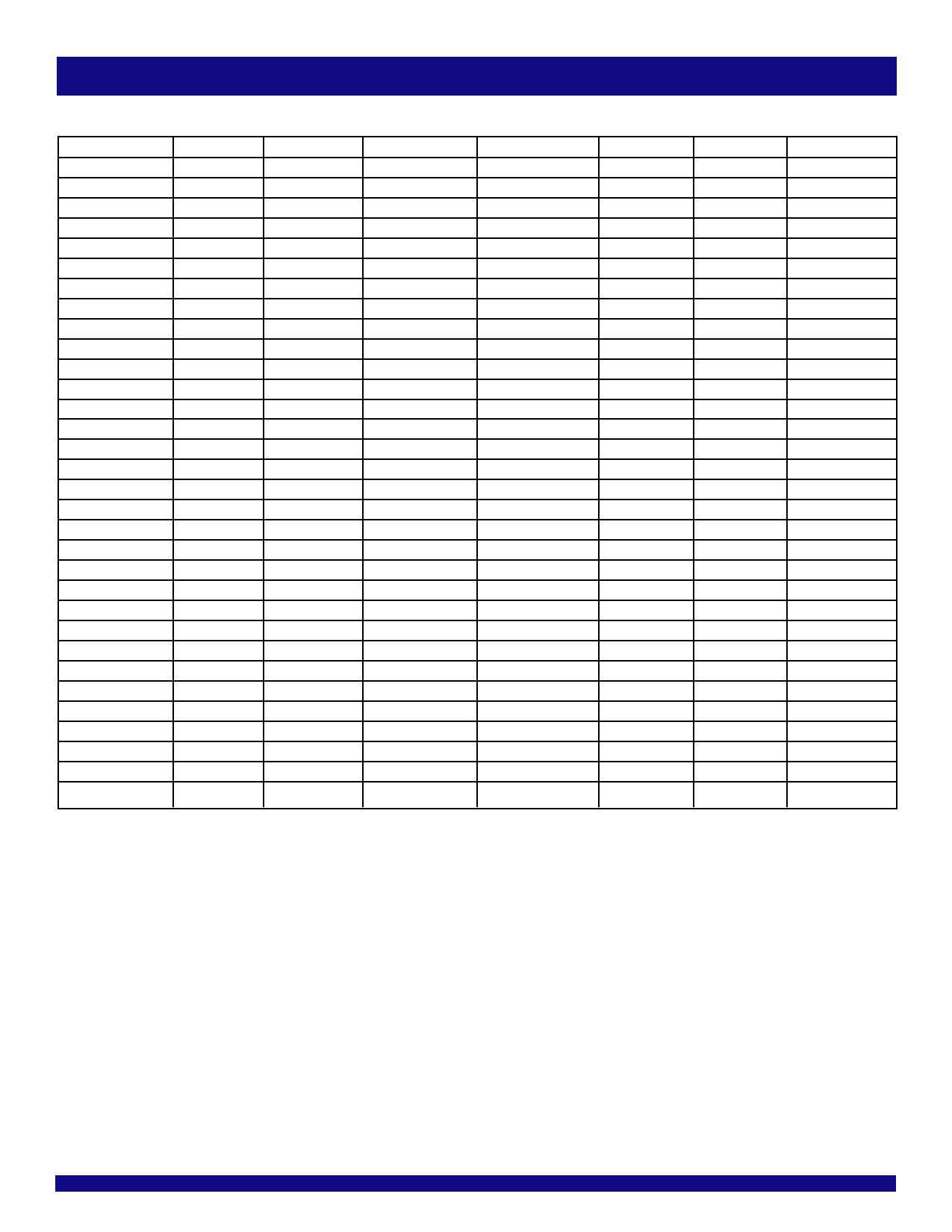
GEAR RATIOS
Select FSA
0
SMBus3
0
00
00
00
00
00
00
00
01
01
01
01
01
01
01
01
10
10
10
10
10
10
10
10
11
11
11
11
11
11
11
11
SMBus2
0
0
0
0
1
1
1
1
0
0
0
0
1
1
1
1
0
0
0
0
1
1
1
1
0
0
0
0
1
1
1
1
SMBus1
0
0
1
1
0
0
1
1
0
0
1
1
0
0
1
1
0
0
1
1
0
0
1
1
0
0
1
1
0
0
1
1
SMBus0
0
1
0
1
0
1
0
1
0
1
0
1
0
1
0
1
0
1
0
1
0
1
0
1
0
1
0
1
0
1
0
1
COMMERCIALTEMPERATURERANGE
m n Gear n/m
31
0.333
52
0.400
12 5
0.417
21
0.500
53
0.600
85
0.625
32
0.667
43
0.750
65
0.833
11
1.000
56
1.200
45
1.250
34
1.333
23
1.500
35
1.667
12
2.000
31
0.333
52
0.400
12 5
0.417
21
0.500
53
0.600
85
0.625
32
0.667
54
0.800
65
0.833
11
1.000
56
1.200
45
1.250
34
1.333
23
1.500
35
1.667
12
2.000
5
Free Datasheet http://www.datasheet4u.com/
5 Page 
IDTCV145
1-TO-19DIFFERENTIALCLOCKBUFFER
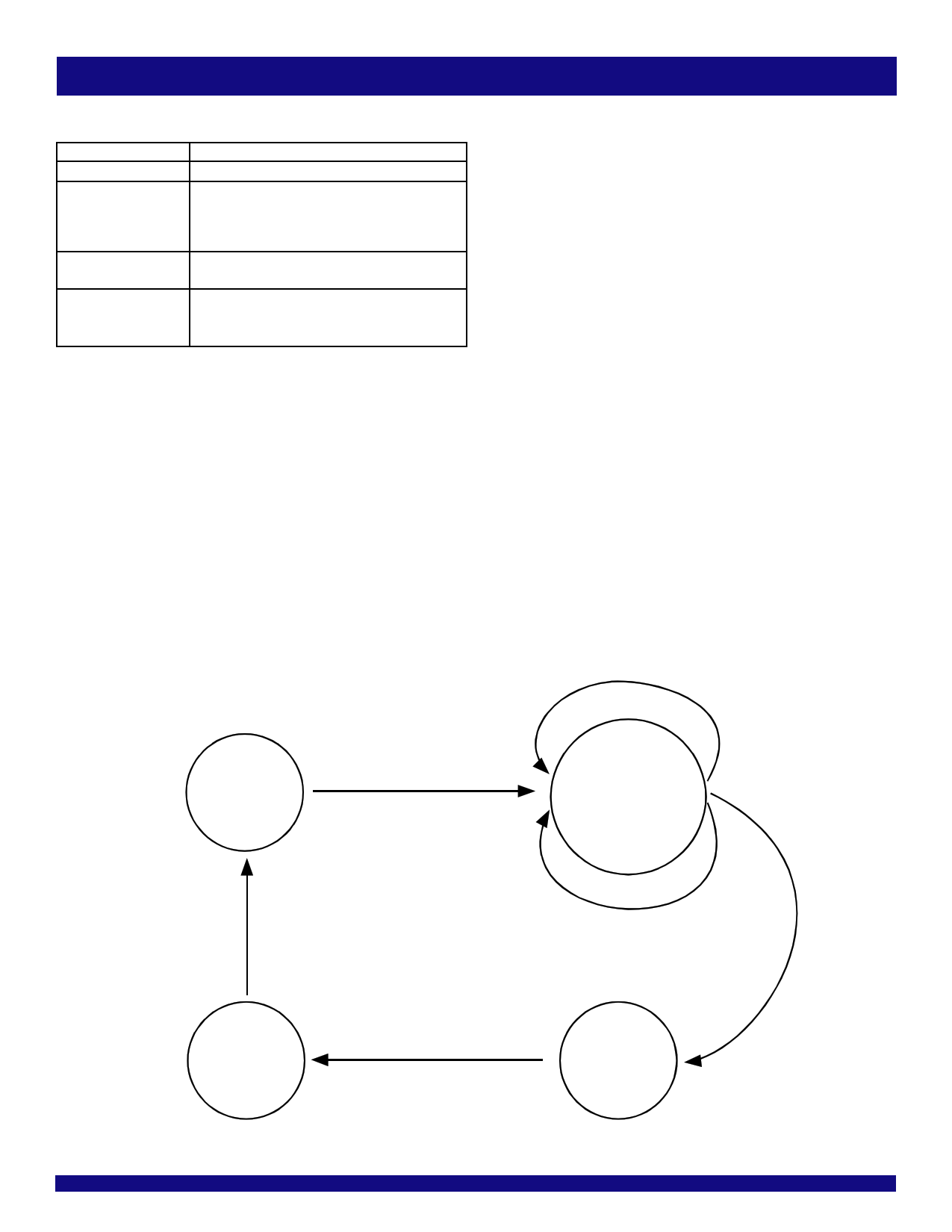
BUFFER POWER-UP STATE MACHINE(1)
State Description
State0
Power off
State1
After 3.3V supply is detected to rise above 1.8-2V, the
bufferentersstate1andinitiatesa0.2ms-0.3msdelay.The
totalpoweruplatencyfrompowerontoalloutputsactive
must be less than 1ms (assume SRC_IN is available)
State2
Buffer waits for a valid clock on the SRC_IN input and
PD de-assertion.
State3
Only after SRC_IN and power valid, PD de-asserted
with the current mirror stable, or PLL lock, the DIF
outputs are enabled
NOTE:
1. The total power up latency from power on to all outputs active must be less than 1ms
(assuming a valid clock is present on CLK_IN input). If power is valid and PWRDWN is
de-asserted but no input clocks are present on the CLK_IN input, DIF clocks must remain
disabled. Only after valid input clocks are detected, valid power, PWRDWN# de-asserted
with the PLL locked/stable and the DIF outputs enabled (doesn't apply to bypass mode).
COMMERCIALTEMPERATURERANGE
BUFFER POWER-UP STATE DIAGRAM
S1
Delay
>0.25 ms
S0
Power Off
No Input Clock
S2
Wait for input
clock and
PWRDWN#
de-assertion
PWRDWN# Asserted
S3
Normal
Operation
11
Free Datasheet http://www.datasheet4u.com/
11 Page | ||
| Páginas | Total 13 Páginas | |
| PDF Descargar | [ Datasheet IDTCV145.PDF ] | |
Hoja de datos destacado
| Número de pieza | Descripción | Fabricantes |
| IDTCV140 | CLOCK | Integrated Device Technology |
| IDTCV144 | CLOCK | Integrated Device Technology |
| IDTCV145 | CLOCK BUFFER | Integrated Device Technology |
| Número de pieza | Descripción | Fabricantes |
| SLA6805M | High Voltage 3 phase Motor Driver IC. |
Sanken |
| SDC1742 | 12- and 14-Bit Hybrid Synchro / Resolver-to-Digital Converters. |
Analog Devices |
|
DataSheet.es es una pagina web que funciona como un repositorio de manuales o hoja de datos de muchos de los productos más populares, |
| DataSheet.es | 2020 | Privacy Policy | Contacto | Buscar |
