|
|
|
PDF ADP5063 Data sheet ( Hoja de datos )
| Número de pieza | ADP5063 | |
| Descripción | Linear LiFePO4 Battery Charger | |
| Fabricantes | Analog Devices | |
| Logotipo | ||
Hay una vista previa y un enlace de descarga de ADP5063 (archivo pdf) en la parte inferior de esta página. Total 30 Páginas | ||
|
No Preview Available !
Data Sheet
Linear LiFePO4 Battery Charger with
Power Path and USB Compatibility in LFCSP
ADP5063
FEATURES
GENERAL DESCRIPTION
Default charging termination voltage at 3.6 V
Fully compatible with USB 3.0 and USB Battery Charging 1.2
Compliance Plan Specification
Operating input voltage from 4 V to 6.7 V
Tolerant input voltage from −0.5 V to +20 V (USB VBUS)
Fully programmable via I2C
Flexible digital control inputs
Up to 2.1 A current from an ac charger in LDO mode
Built-in current sensing and limiting
As low as 55 mΩ battery isolation FET between battery and
charger output
Thermal regulation prevents overheating
Compliant with JEITA1 and JEITA2 Li-Ion battery charging
temperature specifications
SYS_EN flag permits the system to be disabled until battery is at
the minimum required level for guaranteed system start-up
4 mm × 4 mm LFCSP package
APPLICATIONS
Single cell lithium iron phosphate (LiFePO4) portable
equipment
Portable medical devices
Portable instrumentation devices
Portable consumer devices
The ADP5063 charger is fully compliant with USB 3.0 and the
USB Battery Charging 1.2 Compliance Plan Specification, and
enables charging via the mini USB VBUS pin from a wall charger,
car charger, or USB host port.
The ADP5063 operates from a 4 V to 6.7 V input voltage range but
is tolerant of voltages up to 20 V, thereby alleviating concerns about
USB bus spikes during disconnection or connection scenarios.
The ADP5063 features an internal field effect transistor (FET)
between the linear charger output and the battery. This permits
battery isolation and, therefore, system powering under a dead
battery or no battery scenario, which allows immediate system
function upon connection to a USB power supply.
Based on the type of USB source, which is detected by an external
USB detection chip, the ADP5063 can be set to apply the correct
current limit for optimal charging and USB compliance.
The ADP5063 has three factory-programmable digital input/out-
put pins that provide maximum flexibility for different systems.
These digital input/output pins permit a combination of features,
such as input current limits, charging enable and disable, charging
current limits, and a dedicated interrupt output pin.
http://www.DataSheet4U.com/
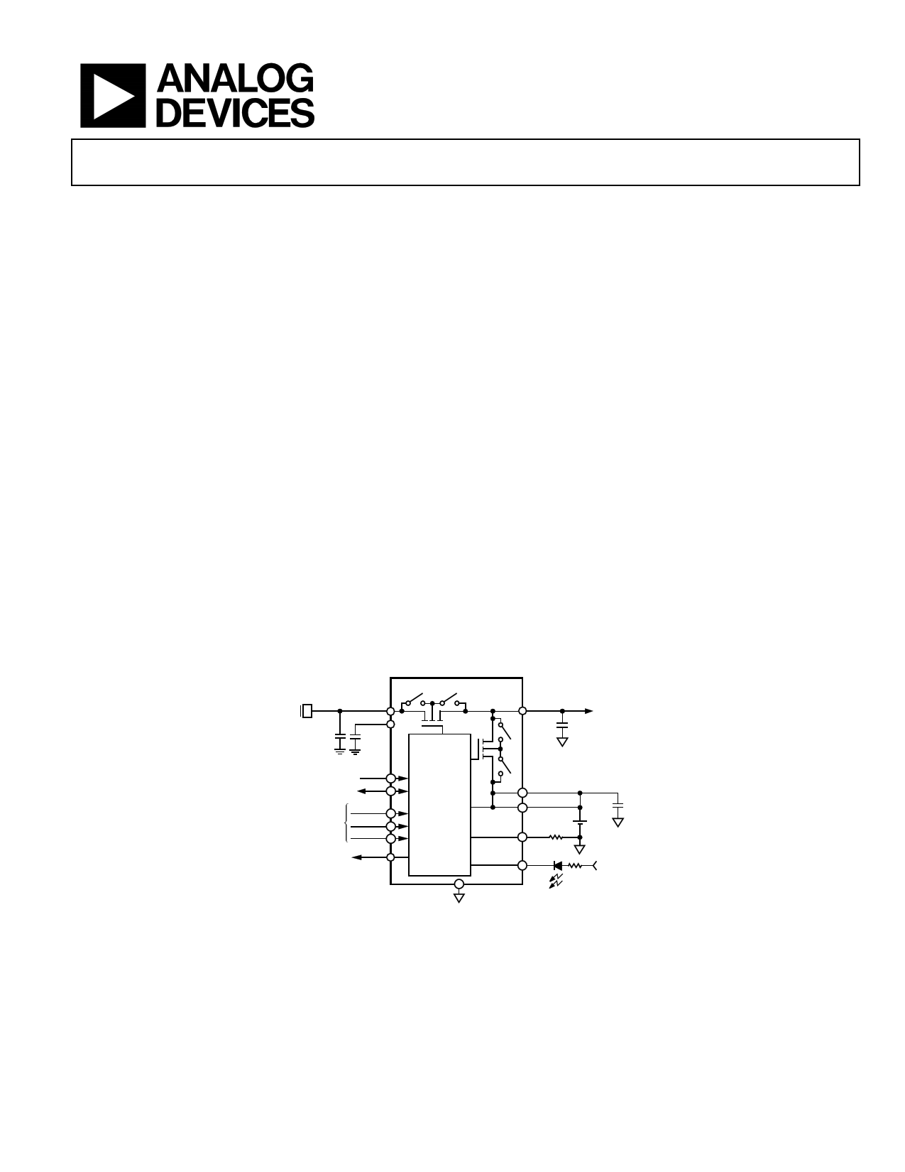
TYPICAL APPLICATION CIRCUIT
AC OR
USB
VBUS
C4
10µF
VINx
CBP
C1
100nF
ADP5063
ISO_Sx SYSTEM
C3
22µF
SCL
SDA
DIG_IO1
DIG_IO2
DIG_IO3
SYS_EN
CHARGER
CONTROL
BLOCK
AGND
Figure 1.
ISO_Bx
BAT_SNS
+ Li-Ion
THR
C2
22µF
ILED
VLED
Rev. 0
Document Feedback
Information furnished by Analog Devices is believed to be accurate and reliable. However, no
responsibility is assumed by Analog Devices for its use, nor for any infringements of patents or other
rights of third parties that may result from its use. Specifications subject to change without notice. No
license is granted by implication or otherwise under any patent or patent rights of Analog Devices.
Trademarksandregisteredtrademarksarethepropertyoftheirrespectiveowners.
One Technology Way, P.O. Box 9106, Norwood, MA 02062-9106, U.S.A.
Tel: 781.329.4700
©2013 Analog Devices, Inc. All rights reserved.
Technical Support
www.analog.com
1 page 
Data Sheet
ADP5063
Parameter
JEITA Hot Temperature
Resistance Thresholds
Hot to Warm Resistance
Warm to Hot Resistance
JEITA2 Li-ION BATTERY CHARGING
SPECIFICATION DEFAULTS
JEITA Cold Temperature
Resistance Thresholds
Cool to Cold Resistance
Cold to Cool Resistance
JEITA Cool Temperature
Resistance Thresholds
Typical to Cool Resistance
Cool to Typical Resistance
JEITA Warm Temperature
Resistance Thresholds
Warm to Typical Resistance
Typical to Warm Resistance
JEITA Hot Temperature
Resistance Thresholds
Hot to Warm Resistance
Warm to Hot Resistance
BATTERY DETECTION
Sink Current
Source Current
Battery Threshold
Low
High
Battery Detection Timer
TIMERS
Clock Oscillator Frequency
Start Charging Delay
Trickle Charge
Fast Charge
Charge Complete
Deglitch
Watchdog2
Safety
Battery Short2
ILED OUTPUT PINS
Voltage Drop over ILED
Maximum Operating Voltage over
ILED
SYS_EN OUTPUT Pin
SYS_EN FET On Resistance
Symbol
TJEITA_HOT
RHOT_FALL
RHOT_RISE
Min
2750
Typ
60
3700
3350
Max
3950
Unit Test Conditions/Comments
°C No battery charging occurs
Ω
Ω
TJEITA_COLD
RCOLD_FALL
RCOLD_RISE
TJEITA_COOL
RTYP_FALL
RTYP_RISE
TJEITA_WARM
RWARM_FALL
RWARM_RISE
TJEITA_HOT
RHOT_FALL
RHOT_RISE
ISINK
ISOURCE
VBATL
VBATH
tBATOK
fCLK
tSTART
tTRK
tCHG
tEND
tDG
tWD
tSAFE
tBAT_SHR
VILED
VMAXILED
0 °C No battery charging occurs
20,500
25,600
24,400
10
30,720
Ω
Ω
°C
Battery termination voltage (VTRM) is reduced by
100 mV
13,200
16,500
15,900
45
19,800
Ω
Ω
°C
Battery termination voltage (VTRM) is reduced by
100 mV
4260
5800
5200
60
6140
Ω
Ω
°C
No battery charging occurs
2750
3700
3350
3950
Ω
Ω
13
7
1.8
20
10
1.9
3.4
333
http://www.DataSheet4U.com/
34
13
2.0
mA
mA
V
V
ms
2.7 3
1
60
600
7.5
31
32
36 40
30
3.3 MHz
sec
min
min
min
VBAT_SNS = VTRM, ICHG < IEND
ms Applies to VTRK_DEAD, VRCH, IEND, VWEAK, V ,VIN_OK_RISE and
VVIN_OK_FALL
sec
44 min
sec
200 mV IILED = 20 mA
5.5 V
RON_SYS_EN
10
Ω ISYS_EN = 20 mA
Rev. 0 | Page 5 of 44
5 Page 
Data Sheet
3.5
DEFAULT STARTUP
DIS_LDO = HIGH
3.0
2.5
2.0
1.5
1.0
0.5
0
2345678
INPUT VOLTAGE (V)
Figure 8. Input Current vs. Input Voltage, VISO_Bx = 3.3 V
70
65
60
55
50
45
40
0 0.5 1.0 1.5
LOAD CURRENT (A)
Figure 9. Ideal Diode RON vs. Load Current,
VISO_Bx = 3.6 V
2.0
ADP5063
3.8 0.6
3.7
0.5
3.6
0.4
3.5
3.4 0.3
3.3
3.2
3.1
3.0
0
VBAT_SNS
IISO_B
20 40 60
CHARGE TIME (Minutes)
0.2
0.1
0
80
Figure 10. Charge Profile, ILIM[3:0] = 0110 (Binary) = 500 mA,
LiFePO4 Battery Capacity = 500 mAh
http://www.DataSheet4U.com/
Rev. 0 | Page 11 of 44
11 Page | ||
| Páginas | Total 30 Páginas | |
| PDF Descargar | [ Datasheet ADP5063.PDF ] | |
Hoja de datos destacado
| Número de pieza | Descripción | Fabricantes |
| ADP5061 | Tiny I2C Programmable Linear Battery Charger | Analog Devices |
| ADP5062 | Linear Li-Ion Battery Charger | Analog Devices |
| ADP5063 | Linear LiFePO4 Battery Charger | Analog Devices |
| ADP5065 | Fast Charge Battery Manager | Analog Devices |
| Número de pieza | Descripción | Fabricantes |
| SLA6805M | High Voltage 3 phase Motor Driver IC. |
Sanken |
| SDC1742 | 12- and 14-Bit Hybrid Synchro / Resolver-to-Digital Converters. |
Analog Devices |
|
DataSheet.es es una pagina web que funciona como un repositorio de manuales o hoja de datos de muchos de los productos más populares, |
| DataSheet.es | 2020 | Privacy Policy | Contacto | Buscar |