|
|
|
PDF CF9501A Data sheet ( Hoja de datos )
| Número de pieza | CF9501A | |
| Descripción | Radio Controlled Clock Receiver IC | |
| Fabricantes | NPC | |
| Logotipo | ||
Hay una vista previa y un enlace de descarga de CF9501A (archivo pdf) en la parte inferior de esta página. Total 10 Páginas | ||
|
No Preview Available !
SM9501A/B
Radio Controlled Clock Receiver IC
OVERVIEW
The SM9501A/B is a BiCMOS RCC*1 receiver IC. It accepts low frequency standard wave input received
from an external antenna, amplifies it, detects the data signal, and outputs a digital time code signal.
*1: Radio controlled clock
FEATURES
I Operating supply voltage range
• 2.4 to 3.6V (A version)
• 4.5 to 5.5V (B version)
I Operating current consumption
• 55µA (typ) @3V (A version)
• 55µA (typ) @5V (B version)
I Standby current consumption
• 0.1µA (max) @3V (A version)
• 0.1µA (max) @5V (B version)
I High sensitivity: 0.5µVrms input
I Wide frequency range (35kHz to 80kHz)
I Include analog switch for antennatuning capaci-
tors change
I AGC gain hold function
I External crystal filter connection
I BiCMOS process
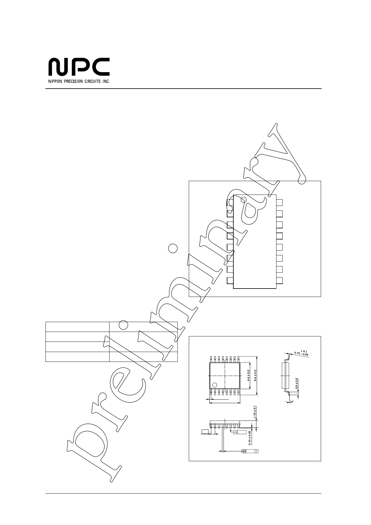
I Package:16-pin VSOP, Chip form
PINOUT
(Top view)
http://www.DataSheet4U.net/
VDDA
IN1
IN3
IN2
FCN
XO
VSSA
XI
1
8
16 VDD
PON
OUT
VSS
HLDN
CP
CB
9 LF
ORDERING INFORMATION
Device
SM9501AV
SM9501BV
CF9501A
Package
16-pin VSOP
Chip form
PACKAGE DIMENSIONS
(Unit: mm)
0.15
+
−
0.1
0.05
0.275TYP
5.1 ± 0.2
0.65 0.10
+ 0.1
0.22 − 0.05
0.12 M
0 to 10 °
NIPPON PRECISION CIRCUITS INC.—1
datasheet pdf - http://www.DataSheet4U.net/
1 page 
SM9501A/B
Electrical Characteristics
9501A version
VDD = 2.4 to 3.6V, VSS = 0V, Ta = −20 to +70°C unless otherwise noted.
Parameter
Symbol
Condition
Minimum operating voltage
Maximum operating voltage
Maximum operating current
consumption1
Operating current consumption1
Standby mode current consumption
Minimum input voltage range
Maximum input voltage range
Input frequency
Analog switch resistance
Startup time2
Startup time2 (PON)
PON input current
FCN input current
HLDN input current
LOW-level output current
HIGH-level output current
Gain hold time
Fall time output propagation delay3
Rise time output propagation delay3
LOW-level output pulsewidth4 (200ms)
LOW-level output pulsewidth4 (500ms)
LOW-level output pulsewidth4 (800ms)
Noise rejection ratio5
VMIN
VMAX
IDDM
IDDT
IST
VFMIN
VFMAX
FIN
RA
tON
tPON
II1
II2
II3
IOL
IOH
tHLD
tDN
tUP
T200
T500
T800
S/N
VDD = 3.0V, no input signal,
PON: VSS, OUT: OPEN
VDD = 3.0V, 500ms pulsewidth,
0.1mVrms input (differential input),
PON: VSS, OUT: OPEN
PON, FCN, HLDN: VDD or OPEN
IN1–IN2 differential input
IN1–IN2 differential input
IN1–IN2 differential input
V|IN2–IN3| = 50mV, VIN2 = 0V
When supply is applied
From standby mode
VIN = 0V
VIN = 0V
VIN = 0V
VDD = 2.4V, OUT = 0.5V
http://www.DataSheet4U.net/
VDD = 2.4V, OUT = 1.9V
± 3dB change
FIN = 40/60kHz, standard crystal,
NPC standard jig
VIN = 1µVrms to 80mVrms
Rating
min typ max
– – 2.4
3.6 –
–
– 65 100
Unit
V
V
µA
– 55 – µA
– – 0.1 µA
– 0.5 1.0 µVrms
80 –
– mVrms
35 – 80 kHz
– – 15 Ω
– – 8 sec
– – 8 sec
– – –1.5 µA
– – –1.5 µA
– – –1.5 µA
10 –
– µA
–10 –
– µA
– – 1 sec
– – 160 ms
– – 200 ms
100 200 300 ms
400 500 650 ms
700 800 900 ms
– – 9 dB
1. Measured using the standard circuit.
2. The time taken under stable wave input conditions from when power is applied or standby is released, using PON, until stable digital output occurs
within ratings.
3. The time taken, with 10:1 input signal amplitude ratio and 500ms pulsewidth, from when a change in signal input occurs until the output OUT changes.
Note that this characteristic is very dependent on the antenna and crystal filter characteristics. The standard crystal used here has the following equiv-
alent circuit coefficients.
L1 C1 R1
f [kHz]
40
60
L1 [kH]
6.70280
5.17396
C1 [fF]
2.36228
1.36007
R1 [kΩ]
11.4492
13.4826
C0 [pF]
1.42773
1.04927
C0
4. Values obtained when using the standard crystal employed here. Note that these values are dependent on the crystal characteristics, and should be
considered as reference values.
5. Time averaged rms values, where the noise is white noise and the measurement bandwidth is determined by the crystal filter equivalent used in the
standard circuit.
NIPPON PRECISION CIRCUITS INC.—5
datasheet pdf - http://www.DataSheet4U.net/
5 Page | ||
| Páginas | Total 10 Páginas | |
| PDF Descargar | [ Datasheet CF9501A.PDF ] | |
Hoja de datos destacado
| Número de pieza | Descripción | Fabricantes |
| CF9501A | Radio Controlled Clock Receiver IC | NPC |
| CF9501B | Radio Controlled Clock Receiver IC | NPC |
| Número de pieza | Descripción | Fabricantes |
| SLA6805M | High Voltage 3 phase Motor Driver IC. |
Sanken |
| SDC1742 | 12- and 14-Bit Hybrid Synchro / Resolver-to-Digital Converters. |
Analog Devices |
|
DataSheet.es es una pagina web que funciona como un repositorio de manuales o hoja de datos de muchos de los productos más populares, |
| DataSheet.es | 2020 | Privacy Policy | Contacto | Buscar |