|
|
|
PDF LTM4620 Data sheet ( Hoja de datos )
| Número de pieza | LTM4620 | |
| Descripción | Dual 13A or Single 26A DC/DC iModule Regulator | |
| Fabricantes | Linear | |
| Logotipo | ||
Hay una vista previa y un enlace de descarga de LTM4620 (archivo pdf) en la parte inferior de esta página. Total 30 Páginas | ||
|
No Preview Available !
LTM4620
Dual 13A or Single 26A
DC/DC µModule Regulator
Features
n Complete Standalone Dual Output Power Supply
n Dual 13A or Single 26A Output
n Wide Input Voltage Range: 4.5V to 16V
n Output Voltage Range: 0.6V to 2.5V
n ±1.5% Maximum Total DC Output Error
n Multiphase Current Sharing with Multiple
LTM4620s Up to 100A
n Differential Remote Sense Amplifier
n Current Mode Control/Fast Transient Response
n Adjustable Switching Frequency
n Overcurrent Foldback Protection
n Frequency Synchronization
n Internal Temperature Sensing Diode Output
n Output Overvoltage Protection
n Low Profile (15mm × 15mm × 4.41mm) LGA Package
Applications
n Telecom and Networking Equipment
n Storage and ATCA Cards
n Industrial Equipment
Video TechClip
Click and Learn
100A and 26A Thermal Performance
Current Sharing
Short-Circuit Protection
Description
The LTM®4620 is a complete dual 13A output switching
mode DC/DC power supply. Included in the package are
the switching controller, power FETs, inductors, and all
supporting components. Operating from an input voltage
range of 4.5V to 16V, the LTM4620 supports two outputs
each with an output voltage range of 0.6V to 2.5V, set by a
single external resistor. Its high efficiency design delivers
up to 13A continuous current for each output. Only a few
input and output capacitors are needed.
The device supports frequency synchronization, multi-
phase operation, Burst Mode operation and output voltage
tracking for supply rail sequencing and has an onboard
temperature diode for device temperature monitoring. High
switching frequency and a current mode architecture enable
a very fast transient response to line and load changes
without sacrificing stability.
Fault protection features include overvoltage and overcur-
rent protection. The power module is offered in a proprietary
spacewww.DataSheet.net/ saving and thermally enhanced 15mm × 15mm ×
4.41mm LGA package with integrated top-side heat sink.
The LTM4620 is RoHS compliant with a PB-free finish.
L, LT, LTC, LTM, Linear Technology, the Linear logo, µModule, Burst Mode and PolyPhase are
registered trademarks and LTpowerCAD is a trademark of Linear Technology Corporation. All
other trademarks are the property of their respective owners.
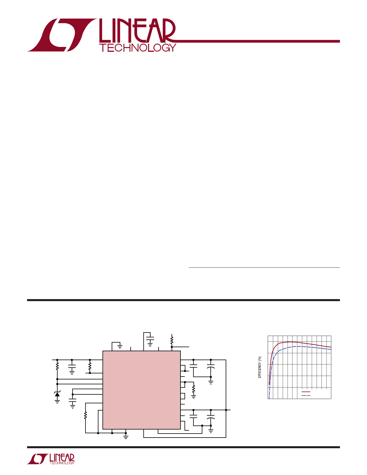
Typical Application
26A, 1.2V Output DC/DC µModule® Regulator
4.7µF
INTVCC
5k
VIN 4.5V TO 16V
10k*
22µF
× 4 120k
25V
5.1V*
0.1µF
121k
* PULL-UP RESISTOR AND
ZENER ARE OPTIONAL
MODE_PLLIN CLKOUT INTVCC
VIN
TEMP
RUN1
RUN2
TRACK1
TRACK2
fSET
PHASMD
LTM4620
SGND GND
DIFFP
EXTVCC PGOOD1
VOUT1
VOUTS1
DIFFOUT
SW1
VFB1
VFB2
COMP1
COMP2
VOUTS2
VOUT2
SW2
PGOOD2
DIFFN
PGOOD
100µF +
6.3V
470µF
6.3V
60.4k
100µF +
6.3V
470µF
6.3V
VOUT
1.2V AT 26A
PGOOD
4620 TA01a
1.2V Efficiency vs IOUT
90
80
70
60
50
5VIN /500kHz
40 12VIN/500kHz
0 2 4 6 8 10 12 14 16 18 20 22 24 26
OUTPUT CURRENT (A)
4620 TA01b
4620f
1
Datasheet pdf - http://www.DataSheet4U.co.kr/
1 page 
Typical Performance Characteristics
Efficiency vs Output Current,
VIN = 5V
100
95
90
85
80
75
70
1VOUT, f = 400kHz
1.2VOUT, f = 500kHz
65
1.5VOUT, f = 550kHz
1.8VOUT, f = 600kHz
60 2.5VOUT, f = 750kHz
0 1 2 3 4 5 6 7 8 9 10 11 12 13
OUTPUT CURRENT (A)
4620 G01
Dual Phase Single Output
Load Transient Response
Efficiency vs Output Current,
VIN = 12V
95
90
85
80
75
70 1VOUT, f = 400kHz
1.2VOUT, f = 500kHz
65
1.5VOUT, f = 550kHz
1.8VOUT, f = 600kHz
60 2.5VOUT, f = 750kHz
0 1 2 3 4 5 6 7 8 9 10 11 12 13
OUTPUT CURRENT (A)
4620 G02
Single Phase Single Output
Load Transient Response
LTM4620
Dual Phase Single Output Efficiency
vs Output Current, VIN = 12V
95
90
85
80
75
70 1VOUT, f = 400kHz
1.2VOUT, f = 500kHz
65
1.5VOUT, f = 550kHz
1.8VOUT, f = 600kHz
60 2.5VOUT, f = 750kHz
0 2 4 6 8 10 12 14 16 18 20 22 24 26
OUTPUT CURRENT (A)
4620 G03
Single Phase Single Output
Load Transient Response
VOUT
100mV/DIV
VOUT
100mV/DIV
VOUT
100mV/DIV
www.DataSheet.net/
ILOAD
10A/DIV
50µs/DIV
12VIN, 1.5VOUT AT 26A/µs LOAD STEP
COUT = 4× 470µF, 4V POSCAP AND
2× 100µF, 6.3V CERAMIC
4620 G04
ILOAD
5A/DIV
50µs/DIV
12VIN, 1VOUT AT 13A/µs LOAD STEP
COUT = 2× 470µF, 4V POSCAP AND
1× 100µF, 6.3V CERAMIC
4620 G05
ILOAD
5A/DIV
50µs/DIV
12VIN, 1.2VOUT AT 13A/µs LOAD STEP
COUT = 2× 470µF, 4V POSCAP AND
1× 100µF, 6.3V CERAMIC
4620 G06
Single Phase Single Output
Load Transient Response
VOUT
100mV/DIV
Single Phase Single Output
Load Transient Response
VOUT
100mV/DIV
Single Phase Single Output
Load Transient Response
VOUT
100mV/DIV
ILOAD
5A/DIV
50µs/DIV
12VIN, 1.5VOUT AT 13A/µs LOAD STEP
COUT = 2× 470µF, 4V POSCAP AND
1× 100µF, 6.3V CERAMIC
4620 G07
ILOAD
5A/DIV
50µs/DIV
12VIN, 1.8VOUT AT 13A/µs LOAD STEP
COUT = 2× 470µF, 4V POSCAP AND
1× 100µF, 6.3V CERAMIC
4620 G08
ILOAD
5A/DIV
50µs/DIV
12VIN, 2.5VOUT AT 13A/µs LOAD STEP
COUT = 2× 470µF, 4V POSCAP AND
1× 100µF, 6.3V CERAMIC
4620 G09
4620f
5
Datasheet pdf - http://www.DataSheet4U.co.kr/
5 Page 
LTM4620
Applications Information
The typical LTM4620 application circuit is shown in
Figure 23. External component selection is primarily
determined by the maximum load current and output
voltage. Refer to Table 4 for specific external capacitor
requirements for particular applications.
VIN to VOUT Step-Down Ratios
There are restrictions in the maximum VIN and VOUT step-
down ratio that can be achieved for a given input voltage.
Each output of the LTM4620 is capable of 98% duty cycle,
but the VIN to VOUT minimum dropout is still shown as a
function of its load current and will limit output current
capability related to high duty cycle on the top side switch.
Minimum on-time tON(MIN) is another consideration in
operating at a specified duty cycle while operating at a
certain frequency due to the fact that tON(MIN) < D/fSW,
where D is duty cycle and fSW is the switching frequency.
tON(MIN) is specified in the electrical parameters as 90ns.
See Note 8 in the Electrical Characteristics section for
output current guideline.
Output Voltage Programming
The PWM controller has an internal 0.6V reference voltage.
As shown in the Block Diagram, a 60.4kΩ internal feedback
resistor connects between the VOUTS1 to VFB1 and VOUTS2
to VFB2. It is very important that these pins be connected
to their respective outputs for proper feedback regulation.
Overvoltage can occur if these VOUTS1 and VOUTS2 pins are
left floating when used as individual regulators, or at least
one of them is used in paralleled regulators. The output
voltage will default to 0.6V with no feedback resistor on
either VFB1 or VFB2. Adding a resistor RFB from VFB pin to
GND programs the output voltage:
VOUT
=
0.6V
•
60.4k + RFB
RFB
Table 1. VFB Resistor Table vs Various Output Voltages
VOUT 0.6V 1.0V 1.2V 1.5V 1.8V
RFB Open 90.9k 60.4k 40.2k 30.2k
2.5V
19.1k
For parallel operation of multiple channels the same feed-
back setting resistor can be used for the parallel design.
This is done by connecting the VOUTS1 to the output as
shown in Figure 2, thus tying one of the internal 60.4k
resistors to the output. All of the VFB pins tie together with
one programming resistor as shown in Figure 2.
In parallel operation, the VFB pins have an IFB current of 20nA
maximum each channel. To reduce output voltage error due
to this current, an additional VOUTS pin can be tied to VOUT,
and an additional RFB resistor can be used to lower the total
Thevenin equivalent resistance seen by this current. For
example in Figure 2, the total Thevenin equivalent resistance
of the VFB pin is (60.4k//RFB), which is 30.2k where RFB is
equal to 60.4k for a 1.2V output. Four phases connected
in parallel equates to a worse case feedback current of
4 • IFB = 80nA maximum. The voltage error is 80nA • 30.2k
= 2.4mV. If VOUTS2 is connected, as shown in Figure 2, to
VOUT, and another 60.4k resistor is connected from VFB2
to ground, then the voltage error is reduced to 1.2mV. If
the voltage error is acceptable then no additional connec-
tions are necessary. The onboard 60.4k resistor is 0.5%
accurate and the VFB resistor can be chosen by the user to
be as accurate as needed. All COMP pins are tied together
for current sharing between the phases. The TRACK pins
can be tied together and a single soft-start capacitor can
bewww.DataSheet.net/ used to soft-start the regulator. The soft-start equa-
tion will need to have the soft-start current parameter
increased by the number of paralleled channels. See the
Output Voltage Tracking section.
COMP1 LTM4620
COMP2
VOUT1
VOUT2
TRACK1
TRACK2
60.4k
60.4k
VOUTS1
VOUTS2
VFB1
VFB2
0.1µF
COMP1 LTM4620
COMP2
60.4k
TRACK1
TRACK2
60.4k
VOUT1
VOUT2
VOUTS1
VOUTS2
VFB1
VFB2
4620 F02
4 PARALLELED OUTPUTS
FOR 1.2V AT 50A
OPTIONAL CONNECTION
OPTIONAL
RFB
60.4k
USE TO LOWER
TOTAL EQUIVALENT
RESISTANCE TO LOWER
IFB VOLTAGE ERROR
RFB
60.4k
Figure 2. 4-Phase Parallel Configurations
4620f
11
Datasheet pdf - http://www.DataSheet4U.co.kr/
11 Page | ||
| Páginas | Total 30 Páginas | |
| PDF Descargar | [ Datasheet LTM4620.PDF ] | |
Hoja de datos destacado
| Número de pieza | Descripción | Fabricantes |
| LTM4620 | Dual 13A or Single 26A DC/DC iModule Regulator | Linear |
| LTM4620A | Dual 13A or Single 26A DC/DC uModule Regulator | Linear Technology |
| LTM4622 | Dual Ultrathin 2.5A Step-Down DC/DC uModule Regulator | Linear Technology |
| LTM4623 | 3A Step-Down DC/DC uModule Regulator | Linear Technology |
| Número de pieza | Descripción | Fabricantes |
| SLA6805M | High Voltage 3 phase Motor Driver IC. |
Sanken |
| SDC1742 | 12- and 14-Bit Hybrid Synchro / Resolver-to-Digital Converters. |
Analog Devices |
|
DataSheet.es es una pagina web que funciona como un repositorio de manuales o hoja de datos de muchos de los productos más populares, |
| DataSheet.es | 2020 | Privacy Policy | Contacto | Buscar |