|
|
|
PDF HMCAD1050-40 Data sheet ( Hoja de datos )
| Número de pieza | HMCAD1050-40 | |
| Descripción | Dual 13/12-Bit 20/40 MSPS A/D Converter | |
| Fabricantes | Hittite | |
| Logotipo | ||
Hay una vista previa y un enlace de descarga de HMCAD1050-40 (archivo pdf) en la parte inferior de esta página. Total 14 Páginas | ||
|
No Preview Available !
v01.0411
Features
• 13-bit resolution
• 20/40 MSPS Maximum Sampling Rate
• Ultra-Low Power Dissipation: 30/55 mW
• 72.5 dB SNR @ 8 MHz FIN
• Internal Reference Circuitry
• 1.8 V Core Supply Voltage
• 1.7 - 3.6 V I/O supply voltage
• Parallel CMOS output
• 9 x 9 mm 64-Pin QFN (LP9E) Package
0 • Dual Channel
Typical Applications
• Handheld Communication, PMR, SDR
• Medical Imaging
• Portable Test Equipment
• Digital Oscilloscopes
• Baseband / IF Communication
• Video Digitizing
• CCD Digitizing
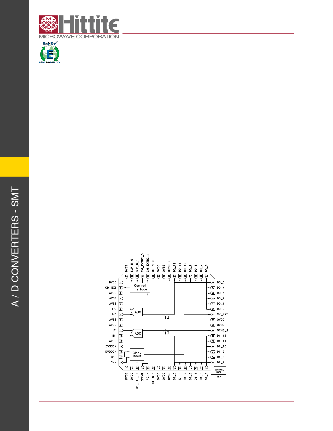
Functional Diagram
HMCAD1050-40
Dual 13/12-Bit 20/40 MSPS
A/D Converter
General Description
The HMCAD1050-40 is a high performance low
power dual analog-to-digital converter (ADC). The
ADC employs internal reference circuitry, a CMOS
control interface, CMOS output data and is based
on a proprietary structure. Digital error correction is
employed to ensure no missing codes in the complete
full scale range.
Several idle modes with fast startup times exist. Each
channel can be independently powered down and
the entire chip can either be put in Standby Mode or
Power Down mode. The different modes are optimized
to allow the user to select the mode resulting in the
lowest possible energy consumption during idle mode
and startup.
The HMCAD1050-40 has a highly linear THA optimized
for frequencies up to 70 MHz. The differential clock
interface is optimized for low jitter clock sources and
supports LVDS, LVPECL, sine wave and CMOS clock
inputs.
Pin compatible with HMCAD1040-40, HMCAD1040-80
and HMCAD1050-80.
www.DataSheet.net/
0-1
Figure 1. Functional Block Diagram
For price, delivery and to place orders: Hittite Microwave Corporation, 2 Elizabeth Drive, Chelmsford, MA 01824
978-250-3343 tel • 978-250-3373 fax • Order On-line at www.hittite.com
Application Support: [email protected]
Datasheet pdf - http://www.DataSheet4U.co.kr/
1 page 
0
v01.0411
HMCAD1050-40
Dual 13/12-Bit 20/40 MSPS
A/D Converter
Digital and Timing Specifications
AVDD= 1.8V, DVDD= 1.8V, DVDDCK= 1.8V, OVDD= 2.5V, Conversion Rate: Max specified, 50% clock duty cycle, -1 dBFS input signal, 5 pF capacitive
load on data outputs, unless otherwise noted
Parameter
Condition
Min
Typ
Max
Unit
Clock Inputs
Duty Cycle
20 80 % high
Compliance
CMOS, LVDS, LVPECL, Sine Wave
Input range
Differential input swing
0.4
Vpp
Input range
Differential input swing, sine wave clock input
1.6
Vpp
Input common mode voltage
Input capacitance
Keep voltages within ground and voltage of OVDD
Differential
0.3
VOVDD -0.3
V
2 pF
Timing
TPD
TSLP
TOVR
TAP
Єrms
Start up time from Power Down Mode to Active Mode
Start up time from Sleep Mode to Active Mode
Out of range recovery time
Aperture Delay
Aperture jitter
1
0.8
< 0.5
900 clock cycles
20 clock cycles
clock cycles
ns
ps
TLAT
TD
TDC
Logic Inputs
Pipeline Delay
Output delay (see timing diagram). 5pF load on output bits
Output delay relative to CK_EXT (see timing diagram)
3
1
12 clock cycles
10 ns
6 ns
VHI
VHI
VLI
VLI
IHI
ILI
CI
Logic Outputs
High Level Input Voltage. VOVDD ≥ 3.0V
High Level Input Voltage. VOVDD = 1.7V – 3.0Vwww.DataSheet.net/
Low Level Input Voltage. VOVDD ≥ 3.0V
Low Level Input Voltage. VOVDD = 1.7V – 3.0V
High Level Input leakage Current
Low Level Input leakage Current
Input Capacitance
2V
0.8 ·VOVDD
0
V
0.8 V
0
0.2 ·VOVDD
V
±10 µA
±10 µA
3 pF
VHO
High Level Output Voltage
VOVDD -0.1
VLO Low Level Output Voltage
CL
Max capacitive load. Post-driver supply voltage equal to digital
supply voltage VOVDD = VDVDD
V
0.1 V
5 pF
CL Max capacitive load. Post-driver supply voltage above 2.25V (1)
10
pF
(1) The outputs will be functional with higher loads. However, it is recommended to keep the load on output data bits as low as possible to keep
dynamic currents and resulting switching noise at a minimum
0-5
For price, delivery and to place orders: Hittite Microwave Corporation, 2 Elizabeth Drive, Chelmsford, MA 01824
978-250-3343 tel • 978-250-3373 fax • Order On-line at www.hittite.com
Application Support: [email protected]
Datasheet pdf - http://www.DataSheet4U.co.kr/
5 Page 
v01.0411
HMCAD1050-40
Dual 13/12-Bit 20/40 MSPS
A/D Converter
always should be lower than the load on data outputs
to ensure sufficient timing margins.
are set, the code is forced to all ones for overrange
and all zeros for underrange.
The digital outputs can be set in tristate mode by set-
Note that the out of range flags (ORNG) will behave
ting the OE_N signal high.
differently for 12 bit and 13 bit output. For 13 bit output
ORNG will be set when digital output data are all ones
The HMCAD1050-40 employs digital offset correc-
or all zeros. For 12-bit output the ORNG flags will be
tion. This means that the output code will be 4096 with
set when all twelve bits are zeros or ones and when
shorted inputs. However, small mismatches in para-
the thirteenth bit is equal to the rest of the bits.
sitics at the input can cause this to alter slightly. The
offset correction also results in possible loss of codes
Data Format Selection
0 at the edges of the full scale range. With no offset
correction, the ADC would clip in one end before the
other, in practice resulting in code loss at the oppo-
site end. With the output being centered digitally, the
output will clip, and the out of range flags will be set,
The output data are presented on offset binary form
when DFRMT is low (connect to OVSS). Setting
DFRMT high (connect to OVDD) results in 2’s comple-
ment output format. Details are shown in table 3.
before max code is reached. When out of range flags
Table 3: Data Format Description for 2Vpp Full Scale Range
Differential Input Voltage (IPx - INx)
Output Data: Dx_12 : Dx_0
(DFRMT = 0, Offset Binary)
1.0 V
1 1111 1111 1111
+0.24mV
-0.24mV
1 0000 0000 0000
www.DataSheet.net/
0 1111 1111 1111
-1.0V
0 0000 0000 0000
Output Data: Dx_12 : Dx_0
(DFRMT = 1, 2’s Complement)
0 1111 1111 1111
0 0000 0000 0000
1 1111 1111 1111
1 0000 0000 0000
The data outputs can be used in three different con-
figurations.
• Normal Mode:
All 13 bits are used. MSB is Dx_12 and LSB is Dx_0.
This mode gives optimum performance
• 12-bit Mode:
The LSB is left unconnected such that only 12 bits
are used. MSB is Dx_12 and LSB is Dx_1. This mode
gives slightly reduced performance due to increased
quantization noise.
Reference Voltages
The reference voltages are internally generated and
buffered based on a bandgap voltage reference. No
external decoupling is necessary, and the reference
voltages are not available externally. This simplifies
usage of the ADC since two extremely sensitive pins,
otherwise needed, are removed from the interface.
If a lower full scale range is required the 13-bit output
word provides sufficient resolution to perform digital
scaling with an equivalent impact on noise compared
to adjusting the reference voltages.
• Reduced Full Scale Range Mode:
The full scale range is reduced from 2 Vpp to 1 Vpp
which is equivalent to 6 dB gain in the ADC frontend.
Note that data are only available in 2’s complement
format in this mode. MSB is Dx_11 and LSB is Dx_0.
Note that the codes will wrap around when exceeding
the full scale range, and that out of range bits should
be used to clamp output data. See section Reference
Voltages for details. This mode gives slightly reduced
performance
A simple way to obtain 1.0Vpp input range with a
12-bit output word is shown in table 4. Note that only
2’s complement output data are available in this mode
and that out of range conditions must be determined
based on a two bit output. The output code will wrap
around when the code goes outside the full scale
range. The out of range bits should be used to clamp
the output data for overrange conditions.
0 - 11
For price, delivery and to place orders: Hittite Microwave Corporation, 2 Elizabeth Drive, Chelmsford, MA 01824
978-250-3343 tel • 978-250-3373 fax • Order On-line at www.hittite.com
Application Support: [email protected]
Datasheet pdf - http://www.DataSheet4U.co.kr/
11 Page | ||
| Páginas | Total 14 Páginas | |
| PDF Descargar | [ Datasheet HMCAD1050-40.PDF ] | |
Hoja de datos destacado
| Número de pieza | Descripción | Fabricantes |
| HMCAD1050-40 | Dual 13/12-Bit 20/40 MSPS A/D Converter | Hittite |
| Número de pieza | Descripción | Fabricantes |
| SLA6805M | High Voltage 3 phase Motor Driver IC. |
Sanken |
| SDC1742 | 12- and 14-Bit Hybrid Synchro / Resolver-to-Digital Converters. |
Analog Devices |
|
DataSheet.es es una pagina web que funciona como un repositorio de manuales o hoja de datos de muchos de los productos más populares, |
| DataSheet.es | 2020 | Privacy Policy | Contacto | Buscar |