|
|
|
PDF 07N60C3 Data sheet ( Hoja de datos )
| Número de pieza | 07N60C3 | |
| Descripción | Power Transistor | |
| Fabricantes | Infineon | |
| Logotipo | ||
 1. - 650V, 7.3A, Power Transistor Hay una vista previa y un enlace de descarga de 07N60C3 (archivo pdf) en la parte inferior de esta página. Total 15 Páginas | ||
|
No Preview Available !
SPP07N60C3
SPI07N60C3, SPA07N60C3
Cool MOS™ Power Transistor
Feature
• New revolutionary high voltage technology
• Ultra low gate charge
VDS @ Tjmax
RDS(on)
ID
650
0.6
7.3
V
Ω
A
• Periodic avalanche rated
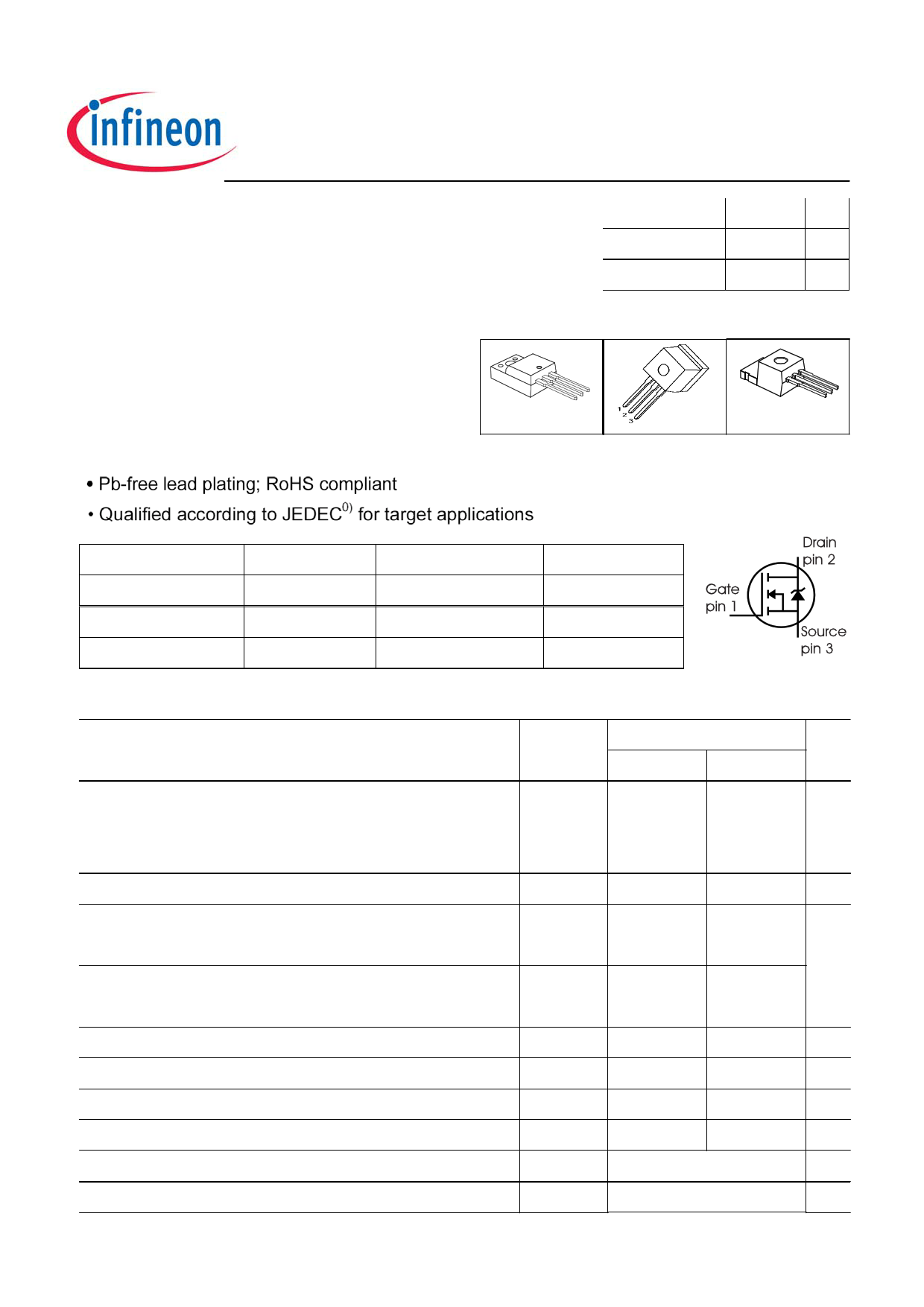
PG-TO220FP PG-TO262
PG-TO220
• Extreme dv/dt rated
2
• High peak current capability
• Improved transconductance
P-TO220-3-31
3
12
• PG-TO-220-3-31;-3-111: Fully isolated package (2500 VAC; 1 minute)
P-TO220-3-1
123
Type
SPP07N60C3
SPI07N60C3
SPA07N60C3
Package
PG-TO220-3
PG-TO262
PG-TO220FP
Ordering Code
Q67040-S4400
Q67040-S4424
SP000216303
Marking
07N60C3
07N60C3
07N60C3
Maximum Ratings
Parameter
Continuous drain current
TC = 25 °C
TC = 100 °C
Pulsed drain current, tp limited by Tjmax
Avalanche energy, single pulse
ID=5.5A, VDD=50V
Avalanche energy, repetitive tAR limited by Tjmax2)
ID=7.3A, VDD=50V
Avalanche current, repetitive tAR limited by Tjmax
Gate source voltage static
Gate source voltage AC (f >1Hz)
Power dissipation, TC = 25°C
Operating and storage temperature
Reverse diode dv/dt 6)
Symbol
ID
ID puls
EAS
EAR
IAR
VGS
VGS
Ptot
Tj , Tstg
dv/dt
Value
SPP_I
SPA
7.3
4.6
21.9
230
7.31)
4.61)
21.9
230
0.5 0.5
7.3 7.3
±20 ±20
±30 ±30
83 32
-55...+150
15
Unit
A
A
mJ
A
V
W
°C
V/ns
Rev. 3.2
Page 1
2009-11-27
1 page 
1 Power dissipation
Ptot = f (TC)
100 SPP07N60C3
W
80
70
60
50
40
30
20
10
00 20 40 60 80 100 120 °C 160
TC
3 Safe operating area
ID = f ( VDS )
parameter : D = 0 , TC=25°C
10 2
A
SPP07N60C3
SPI07N60C3, SPA07N60C3
2 Power dissipation FullPAK
Ptot = f (TC)
34
W
28
24
20
16
12
8
4
00 20 40 60 80 100 120 °C 160
TC
4 Safe operating area FullPAK
ID = f (VDS)
parameter: D = 0, TC = 25°C
10 2
A
10 1
10 1
10 0
10 -1
10
-2
10
0
Rev. 3.2
10 0
tp = 0.001 ms
tp = 0.01 ms
tp = 0.1 ms
tp = 1 ms
DC
10 1
10 2
10 -1
V 10 3
VDS
10
-2
10
0
Page 5
tp = 0.001 ms
tp = 0.01 ms
tp = 0.1 ms
tp = 1 ms
tp = 10 ms
DC
10 1
10 2 V 10 3
VDS
2009-11-27
5 Page 
25 Typ. Coss stored energy
Eoss=f(VDS)
5.5
µJ
4.5
4
3.5
3
2.5
2
1.5
1
0.5
00
100 200 300 400
V
600
VDS
Definition of diodes switching characteristics
SPP07N60C3
SPI07N60C3, SPA07N60C3
Rev. 3.2
Page 11
2009-11-27
11 Page | ||
| Páginas | Total 15 Páginas | |
| PDF Descargar | [ Datasheet 07N60C3.PDF ] | |
Hoja de datos destacado
| Número de pieza | Descripción | Fabricantes |
| 07N60C2 | SPA07N60C2 | Infineon Technologies |
| 07N60C3 | Power Transistor | Infineon |
| Número de pieza | Descripción | Fabricantes |
| SLA6805M | High Voltage 3 phase Motor Driver IC. |
Sanken |
| SDC1742 | 12- and 14-Bit Hybrid Synchro / Resolver-to-Digital Converters. |
Analog Devices |
|
DataSheet.es es una pagina web que funciona como un repositorio de manuales o hoja de datos de muchos de los productos más populares, |
| DataSheet.es | 2020 | Privacy Policy | Contacto | Buscar |