|
|
|
PDF FAN5403 Data sheet ( Hoja de datos )
| Número de pieza | FAN5403 | |
| Descripción | (FAN5401 - FAN5405) USB-Compliant Single-Cell Li-Ion Switching Charger | |
| Fabricantes | Fairchild Semiconductor | |
| Logotipo | ||
Hay una vista previa y un enlace de descarga de FAN5403 (archivo pdf) en la parte inferior de esta página. Total 37 Páginas | ||
|
No Preview Available !
www.DataSheet.co.kr
September 2011
FAN5400/FAN5401/FAN5402/ FAN5403/ FAN5404/ FAN5405
USB-Compliant Single-Cell Li-Ion Switching Charger with
USB-OTG Boost Regulator
Features
Fully Integrated, High-Efficiency Charger for Single-Cell
Li-Ion and Li-Polymer Battery Packs
Faster Charging than Linear
Charge Voltage Accuracy: 0.5% at 25°C
1% from 0 to 125°C
5% Input Current Regulation Accuracy
5% Charge Current Regulation Accuracy
20V Absolute Maximum Input Voltage
6V Maximum Input Operating Voltage
1.25A Maximum Charge Rate
Programmable through High-Speed I2C Interface
(3.4Mb/s) with Fast Mode Plus Compatibility
– Input Current
– Fast-Charge / Termination Current
– Charger Voltage
– Termination Enable
3MHz Synchronous Buck PWM Controller with Wide
Duty Cycle Range
Small Footprint 1H External Inductor
Safety Timer with Reset Control
1.8V Regulated Output from VBUS for Auxiliary Circuits
Weak Input Sources Accommodated by Reducing
Charging Current to Maintain Minimum VBUS Voltage
Low Reverse Leakage to Prevent Battery Drain to VBUS
5V, 300mA Boost Mode for USB OTG for 2.5 to 4.5V
Battery Input
Applications
Cell Phones, Smart Phones, PDAs
Tablet, Portable Media Players
Gaming Device, Digital Cameras
Description
The FAN5400 family (FAN540X) combines a highly integrated
switch-mode charger, to minimize single-cell Lithium-ion
(Li-ion) charging time from a USB power source, and a boost
regulator to power a USB peripheral from the battery.
The charging parameters and operating modes are
programmable through an I2C Interface that operates up to
3.4Mbps. The charger and boost regulator circuits switch at
3MHz to minimize the size of external passive components.
The FAN540X provides battery charging in three phases:
conditioning, constant current, and constant voltage.
To ensure USB compliance and minimize charging time, the
input current is limited to the value set through the I2C host.
Charge termination is determined by a programmable
minimum current level. A safety timer with reset control
provides a safety backup for the I2C host.
The integrated circuit (IC) automatically restarts the charge
cycle when the battery falls below an internal threshold. If the
input source is removed, the IC enters a high-impedance
mode with leakage from the battery to the input prevented.
Charge status is reported back to the host through the I2C
port. Charge current is reduced when the die temperature
reaches 120°C.
The FAN540X can operate as a boost regulator on
command from the system. The boost regulator includes a
soft-start that limits inrush current from the battery.
The FAN540X is available in a 1.96 x 1.87mm, 20-bump,
0.4mm pitch WLCSP package.
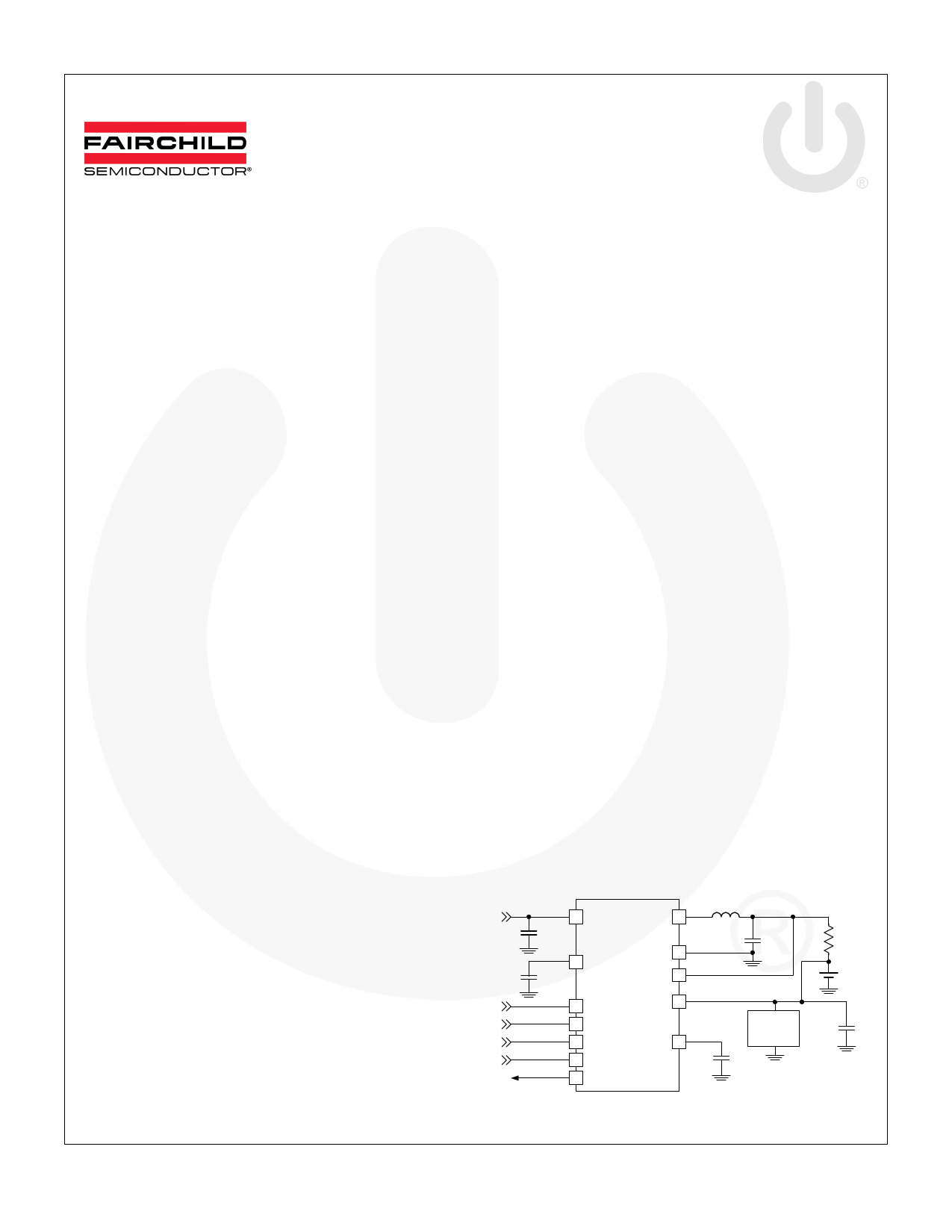
VBUS
CBUS
1F
PMID
CMID
4.7F
SDA
SCL
DISABLE
OTG/USB#
STAT
FAN540X
SW L1 1H
PGND COUT
CSIN
0.1F
RSENSE
68m
+ Battery
VBAT
VREG
CREG
SYSTEM
LOAD
1F
CBAT
10F
All trademarks are the property of their respective owners.
Figure 1. Typical Application (FAN5403-05 Pin Out)
© 2009 Fairchild Semiconductor Corporation
FAN5400 Family • Rev. 1.0.7
www.fairchildsemi.com
Datasheet pdf - http://www.DataSheet4U.net/
1 page 
www.DataSheet.co.kr
Absolute Maximum Ratings
Stresses exceeding the absolute maximum ratings may damage the device. The device may not function or be operable above
the recommended operating conditions and stressing the parts to these levels is not recommended. In addition, extended
exposure to stresses above the recommended operating conditions may affect device reliability. The absolute maximum
ratings are stress ratings only.
Symbol
Parameter
VBUS VBUS Voltage
Continuous
Pulsed, 100ms Maximum Non-Repetitive
VSTAT
VI
STAT Voltage
PMID Voltage
SW, CSIN, VBAT, AUXPWR, DISABLE Voltage
VO Voltage on Other Pins
dVBUS
dt
Maximum VBUS Slope above 5.5V when Boost or Charger are Active
ESD
Electrostatic Discharge
Protection Level
Human Body Model per JESD22-A114
Charged Device Model per JESD22-C101
TJ
TSTG
TL
Junction Temperature
Storage Temperature
Lead Soldering Temperature, 10 Seconds
Note:
3. Lesser of 6.5V or VI + 0.3V.
Min.
–1.4
–2.0
–0.3
–0.3
–0.3
Max.
20.0
16.0
7.0
7.0
6.5(3)
4
2000
500
–40 +150
–65 +150
+260
Unit
V
V
V
V
V/s
V
°C
°C
°C
Recommended Operating Conditions
The Recommended Operating Conditions table defines the conditions for actual device operation. Recommended operating
conditions are specified to ensure optimal performance to the datasheet specifications. Fairchild does not recommend
exceeding them or designing to absolute maximum ratings.
Symbol
VBUS
VBAT(MAX)
dVBUS
dt
TA
TJ
Parameter
Supply Voltage
Maximum Battery Voltage when Boost enabled
Negative VBUS Slew Rate during VBUS Short Circuit,
CMID < 4.7F, see VBUS Short While Charging
Ambient Temperature
TA < 60°C
TA > 60°C
Junction Temperature (see Thermal Regulation and Protection section)
Min.
4
–30
–30
Max.
6
4.5
4
2
+85
+120
Units
V
V
V/s
°C
°C
Thermal Properties
Junction-to-ambient thermal resistance is a function of application and board layout. This data is measured with four-layer
2s2p boards in accordance to JEDEC standard JESD51. Special attention must be paid not to exceed junction temperature
TJ(max) at a given ambient temperature TA. For measured data, see Table 11.
Symbol
JA
JB
Parameter
Junction-to-Ambient Thermal Resistance
Junction-to-PCB Thermal Resistance
Typical
60
20
Units
°C/W
°C/W
© 2009 Fairchild Semiconductor Corporation
FAN5400 Family • Rev. 1.0.7
5
www.fairchildsemi.com
Datasheet pdf - http://www.DataSheet4U.net/
5 Page 
www.DataSheet.co.kr
Charge Mode Typical Characteristics
Unless otherwise specified, circuit of Figure 1, VOREG=4.2V, VBUS=5.0V, and TA=25°C.
180 900
160 800
140 700
120 600
100 500
80 400
60 300
40
20
-
2.5
5.5VBUS
5.0VBUS
4.5VBUS
3 3.5
Battery Voltage, VBAT (V)
4
4.5
200
100
-
2.5
5.5VBUS
5.0VBUS
4.5VBUS
3 3.5
Battery Voltage, VBAT (V)
4
4.5
Figure 7. Battery Charge Current vs. VBUS with
IINLIM=100mA
Figure 8. Battery Charge Current vs. VBUS with IINLIM=500mA
94%
94%
92%
92%
90%
90%
88%
86%
84%
550
4.20VBAT, 4.5VBUS
4.20VBAT, 5.0VBUS
3.54VBAT, 5.0VBUS
3.54VBAT, 4.5VBUS
650 750 850 950 1050
VBAT Load Current (mA)
1150
1250
Figure 9. Charger Efficiency, No IINLIM, IOCHARGE=1,250mA
88%
86%
4.5VBUS
5.0VBUS
84%
5.5VBUS
2.5 2.7 2.9 3.1 3.3 3.5 3.7 3.9 4.1 4.3
Battery Voltage, VBAT (V)
Figure 10. Charger Efficiency vs. VBUS, IINLIM=500mA
Figure 11. Auto-Charge Startup at VBUS Plug-in,
IINLIM=100mA, OTG=1, VBAT=3.4V
Figure 12. Auto-Charge Startup at VBUS Plug-in,
IINLIM=500mA, OTG=1, VBAT=3.4V
© 2009 Fairchild Semiconductor Corporation
FAN5400 Family • Rev. 1.0.7
11
www.fairchildsemi.com
Datasheet pdf - http://www.DataSheet4U.net/
11 Page | ||
| Páginas | Total 37 Páginas | |
| PDF Descargar | [ Datasheet FAN5403.PDF ] | |
Hoja de datos destacado
| Número de pieza | Descripción | Fabricantes |
| FAN5400 | USB-Compliant Single Cell Li-Ion Switching Charger | Fairchild Semiconductor |
| FAN5400 | (FAN5401 - FAN5405) USB-Compliant Single-Cell Li-Ion Switching Charger | Fairchild Semiconductor |
| FAN5401 | (FAN5401 - FAN5405) USB-Compliant Single-Cell Li-Ion Switching Charger | Fairchild Semiconductor |
| FAN54010 | (FAN54010 - FAN54015) USB-Compliant Single Cell Li-Ion Switching Charger | Fairchild Semiconductor |
| Número de pieza | Descripción | Fabricantes |
| SLA6805M | High Voltage 3 phase Motor Driver IC. |
Sanken |
| SDC1742 | 12- and 14-Bit Hybrid Synchro / Resolver-to-Digital Converters. |
Analog Devices |
|
DataSheet.es es una pagina web que funciona como un repositorio de manuales o hoja de datos de muchos de los productos más populares, |
| DataSheet.es | 2020 | Privacy Policy | Contacto | Buscar |