No Preview Available !

www.DataSheet.co.kr
MACH 4 CPLD Family
High Performance E2CMOS®
In-System Programmable Logic
FEATURES
x High-performance, E2CMOS 3.3-V & 5-V CPLD families
x Flexible architecture for rapid logic designs
— Excellent First-Time-FitTM and refit feature
— SpeedLockingTM performance for guaranteed fixed timing
— Central, input and output switch matrices for 100% routability and 100% pin-out retention
x High speed
— 7.5ns tPD Commercial and 10ns tPD Industrial
— 111.1MHz fCNT
x 32 to 256 macrocells; 32 to 384 registers
x 44 to 256 pins in PLCC, PQFP, TQFP and BGA packages
x Flexible architecture for a wide range of design styles
— D/T registers and latches
— Synchronous or asynchronous mode
— Dedicated input registers
— Programmable polarity
— Reset/ preset swapping
x Advanced capabilities for easy system integration
— 3.3-V & 5-V JEDEC-compliant operations
— JTAG (IEEE 1149.1) compliant for boundary scan testing
— 3.3-V & 5-V JTAG in-system programming
— PCI compliant (-7/-10/-12 speed grades)
— Safe for mixed supply voltage system designs
— Bus-FriendlyTM inputs and I/Os
— Programmable security bit
— Individual output slew rate control
x Advanced E2CMOS process provides high-performance, cost-effective solutions
x Supported by ispDesignEXPERTTM software for rapid logic development
— Supports HDL design methodologies with results optimized for MACH 4
— Flexibility to adapt to user requirements
— Software partnerships that ensure customer success
x Lattice and third-party hardware programming support
— LatticePROTM software for in-system programmability support on PCs and automated test
equipment
— Programming support on all major programmers including Data I/O, BP Microsystems, Advin,
and System General
Publication# 17466 Rev: M
Amendment/0
Issue Date: March 2000
Datasheet pdf - http://www.DataSheet4U.net/

www.DataSheet.co.kr
FUNCTIONAL DESCRIPTION
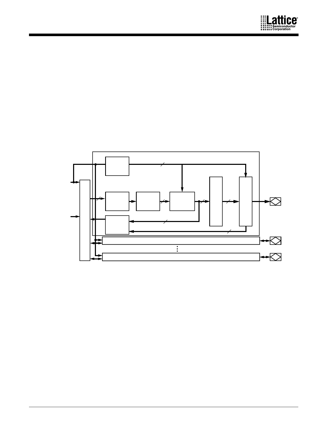
The fundamental architecture of MACH 4 devices (Figure 1) consists of multiple, optimized PAL®
blocks interconnected by a central switch matrix. The central switch matrix allows
communication between PAL blocks and routes inputs to the PAL blocks. Together, the PAL
blocks and central switch matrix allow the logic designer to create large designs in a single
device instead of having to use multiple devices.
The key to being able to make effective use of these devices lies in the interconnect schemes.
In MACH 4 architecture, the macrocells are flexibly coupled to the product terms through the
logic allocator, and the I/O pins are flexibly coupled to the macrocells due to the output switch
matrix. In addition, more input routing options are provided by the input switch matrix. These
resources provide the flexibility needed to fit designs efficiently.
Clock/Input
Pins
Note 3
Dedicated
Input Pins
Clock
Generator
4
Note 2
PAL Block
33/
34/
36
Logic
Array
Input
Switch
Matrix
Logic 16 Output/ 16
Allocator
Buried
with XOR
Macrocells
16
PAL Block
8
Note 1
16
I/O
Pins
I/O
Pins
PAL Block
Figure 1. MACH 4 Block Diagram and PAL Block Structure
I/O
Pins
17466G-001
Notes:
1. 16 for MACH 4 devices with 1:1 macrocell-I/O cell ratio (see next page).
2. Block clocks do not go to I/O cells in M4(LV)-32/32.
3. M4(LV)-192/96 and M4(LV)-256/128 have dedicated clock pins which cannot be used as inputs and do not connect to the central
switch matrix.
MACH 4 Family
5
Datasheet pdf - http://www.DataSheet4U.net/

www.DataSheet.co.kr
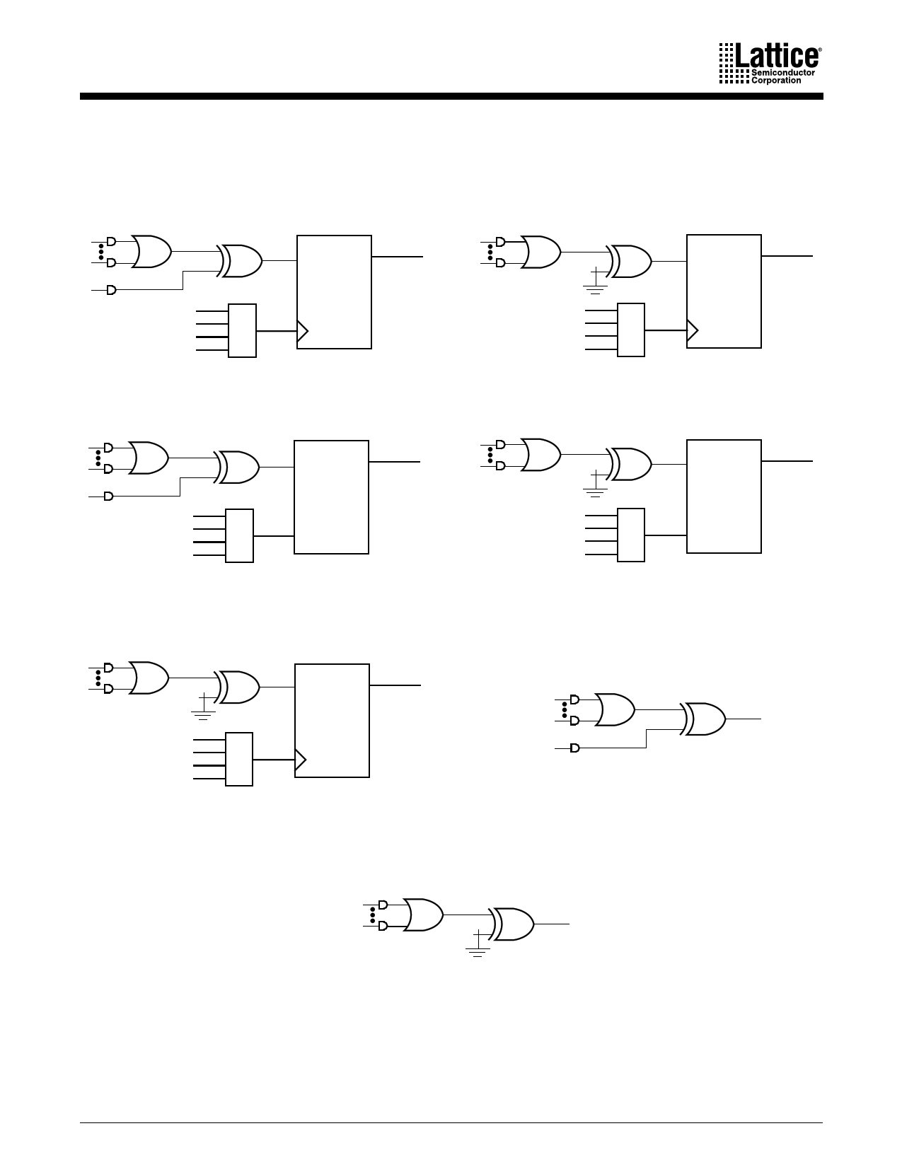
The flip-flop can be configured as a D-type or T-type latch. J-K or S-R registers can be
synthesized. The primary flip-flop configurations are shown in Figure 6, although others are
possible. Flip-flop functionality is defined in Table 8. Note that a J-K latch is inadvisable as it will
cause oscillation if both J and K inputs are HIGH.
AP AR
DQ
AP AR
DQ
a. D-type with XOR
AP AR
LQ
G
c. Latch with XOR
AP AR
TQ
e. T-type with programmable T polarity
b. D-type with programmable D polarity
AP AR
LQ
G
d. Latch with programmable D polarity
f. Combinatorial with XOR
g. Combinatorial with programmable polarity
Figure 6. Primary Macrocell Configurations
MACH 4 Family
17466G-011
11
Datasheet pdf - http://www.DataSheet4U.net/


