|
|
|
PDF IRF540S Data sheet ( Hoja de datos )
| Número de pieza | IRF540S | |
| Descripción | Power MOSFET ( Transistor ) | |
| Fabricantes | Vishay Siliconix | |
| Logotipo | ||
Hay una vista previa y un enlace de descarga de IRF540S (archivo pdf) en la parte inferior de esta página. Total 9 Páginas | ||
|
No Preview Available !
www.DataSheet.co.kr
IRF540S, SiHF540S
Vishay Siliconix
Power MOSFET
PRODUCT SUMMARY
VDS (V)
RDS(on) ()
Qg (Max.) (nC)
Qgs (nC)
Qgd (nC)
Configuration
100
VGS = 10 V
72
11
32
Single
0.077
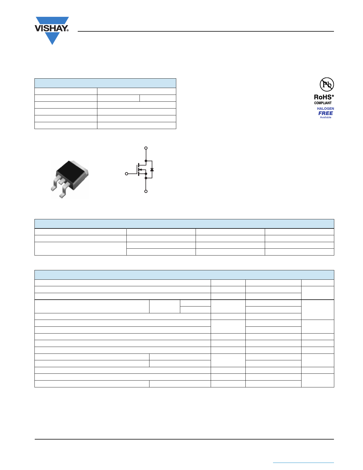
D2PAK (TO-263)
D
G
GD
S
S
N-Channel MOSFET
ORDERING INFORMATION
Package
Lead (Pb)-free and Halogen-free
Lead (Pb)-free
Note
a. See device orientation.
D2PAK (TO-263)
SiHF540S-GE3
IRF540SPbF
SiHF540S-E3
FEATURES
• Halogen-free According to IEC 61249-2-21
Definition
• Surface Mount
• Available in Tape and Reel
• Dynamic dV/dt Rating
• Repetitive Avalanche Rated
• 175 °C Operating Temperature
• Fast Switching
• Ease of Paralleling
• Compliant to RoHS Directive 2002/95/EC
DESCRIPTION
Third generation Power MOSFETs from Vishay provide the
designer with the best combination of fast switching,
ruggedized device design, low on-resistance and
cost-effectiveness.
The D2PAK (TO-263) is a surface mount power package
capable of accommodating die size up to HEX-4. It provides
the highest power capability and the lowest possible
on-resistance in any existing surface mount package. The
D2PAK (TO-263) is suitable for high current applications
because of its low internal connection resistance and can
dissipate up to 2.0 W in a typical surface mount application.
D2PAK (TO-263)
SiHF540STRL-GE3a
IRF540STRLPbFa
SiHF540STL-E3a
D2PAK (TO-263)
SiHF540STRR-GE3a
IRF540STRRPbFa
SiHF540STR-E3a
ABSOLUTE MAXIMUM RATINGS TC = 25 °C, unless otherwise noted
PARAMETER
SYMBOL
Drain-Source Voltage
Gate-Source Voltage
Continuous Drain Current
Pulsed Drain Currenta
Linear Derating Factor
Linear Derating Factor (PCB Mount)e
Single Pulse Avalanche Energyb
Avalanche Currenta
Repetitive Avalanche Energya
Maximum Power Dissipation
Maximum Power Dissipation (PCB Mount)e
Peak Diode Recovery dV/dtc
VGS at 10 V
TC = 25 °C
TC = 100 °C
VDS
VGS
ID
IDM
TC = 25 °C
TA = 25 °C
EAS
IAR
EAR
PD
dV/dt
Operating Junction and Storage Temperature Range
Soldering Recommendations (Peak Temperature)
for 10 s
TJ, Tstg
Notes
a. Repetitive rating; pulse width limited by maximum junction temperature (see fig. 11).
b. VDD = 25 V, starting TJ = 25 °C, L = 440 μH, Rg = 25 , IAS = 28 A (see fig. 12).
c. ISD 28 A, dI/dt 170 A/μs, VDD VDS, TJ 175 °C.
d. 1.6 mm from case.
e. When mounted on 1" square PCB (FR-4 or G-10 material).
LIMIT
100
± 20
28
20
110
1.0
0.025
230
28
15
150
3.7
5.5
- 55 to + 175
300d
UNIT
V
A
W/°C
mJ
A
mJ
W
V/ns
°C
* Pb containing terminations are not RoHS compliant, exemptions may apply
Document Number: 91022
S11-1046-Rev. D, 30-May-11
www.vishay.com
1
This document is subject to change without notice.
THE PRODUCTS DESCRIBED HEREIN AND THIS DOCUMENT ARE SUBJECT TO SPECIFIC DISCLAIMERS, SET FORTH AT www.vishay.com/doc?91000
Datasheet pdf - http://www.DataSheet4U.net/
1 page 
www.DataSheet.co.kr
30
25
20
15
10
5
0
25
91022_09
50 75 100 125 150
TC, Case Temperature (°C)
175
Fig. 9 - Maximum Drain Current vs. Case Temperature
IRF540S, SiHF540S
Vishay Siliconix
VDS
VGS
Rg
RD
D.U.T.
10 V
Pulse width ≤ 1 µs
Duty factor ≤ 0.1 %
+- VDD
Fig. 10a - Switching Time Test Circuit
VDS
90 %
10 %
VGS
td(on) tr
td(off) tf
Fig. 10b - Switching Time Waveforms
10
1
D = 0.5
0.2
0.1 0.1
0.05
0.02
0.01
10-2
10-5
91022_11
Single Pulse
(Thermal Response)
10-4 10-3 10-2 0.1
t1, Rectangular Pulse Duration (s)
PDM
t1
t2
Notes:
1. Duty Factor, D = t1/t2
2. Peak Tj = PDM x ZthJC + TC
1 10
Fig. 11 - Maximum Effective Transient Thermal Impedance, Junction-to-Case
Document Number: 91022
S11-1046-Rev. D, 30-May-11
www.vishay.com
5
This document is subject to change without notice.
THE PRODUCTS DESCRIBED HEREIN AND THIS DOCUMENT ARE SUBJECT TO SPECIFIC DISCLAIMERS, SET FORTH AT www.vishay.com/doc?91000
Datasheet pdf - http://www.DataSheet4U.net/
5 Page | ||
| Páginas | Total 9 Páginas | |
| PDF Descargar | [ Datasheet IRF540S.PDF ] | |
Hoja de datos destacado
| Número de pieza | Descripción | Fabricantes |
| IRF540 | Power MOSFET ( Transistor ) | Vishay |
| IRF540 | N-Channel Power MOSFETs | Harris |
| IRF540 | N-Channel MOSFET Transistor | Inchange Semiconductor |
| IRF540 | N-channel TrenchMOS transistor | NXP Semiconductors |
| Número de pieza | Descripción | Fabricantes |
| SLA6805M | High Voltage 3 phase Motor Driver IC. |
Sanken |
| SDC1742 | 12- and 14-Bit Hybrid Synchro / Resolver-to-Digital Converters. |
Analog Devices |
|
DataSheet.es es una pagina web que funciona como un repositorio de manuales o hoja de datos de muchos de los productos más populares, |
| DataSheet.es | 2020 | Privacy Policy | Contacto | Buscar |