|
|
|
PDF FM24W256 Data sheet ( Hoja de datos )
| Número de pieza | FM24W256 | |
| Descripción | 256Kb Wide Voltage Serial F-RAM | |
| Fabricantes | Ramtron | |
| Logotipo | ||
Hay una vista previa y un enlace de descarga de FM24W256 (archivo pdf) en la parte inferior de esta página. Total 13 Páginas | ||
|
No Preview Available !
www.DataSheet.co.kr
Preliminary
FM24W256
256Kb Wide Voltage Serial F-RAM
Features
256K bit Ferroelectric Nonvolatile RAM
Organized as 32,768 x 8 bits
High Endurance 100 Trillion (1014) Read/Writes
38 year Data Retention (@ +75ºC)
NoDelay™ Writes
Advanced High-Reliability Ferroelectric Process
Fast Two-wire Serial Interface
Up to 1 MHz maximum bus frequency
Direct hardware replacement for EEPROM
Supports legacy timing for 100 kHz & 400 kHz
Description
The FM24W256 is a 256-kilobit nonvolatile memory
employing an advanced ferroelectric process. A
ferroelectric random access memory or F-RAM is
nonvolatile and performs reads and writes like a
RAM. It provides reliable data retention for 10 years
while eliminating the complexities, overhead, and
system level reliability problems caused by
EEPROM and other nonvolatile memories.
The FM24W256 performs write operations at bus
speed. No write delays are incurred. Data is written to
the memory array immediately after it has been
successfully transferred to the device. The next bus
cycle may commence immediately without the need
for data polling. In addition, the product offers
substantial write endurance compared with other
nonvolatile memories. The FM24W256 is capable of
supporting 1014 read/write cycles, or 100 million
times more write cycles than EEPROM.
These capabilities make the FM24W256 ideal for
nonvolatile memory applications requiring frequent
or rapid writes. Examples range from data collection
where the number of write cycles may be critical, to
demanding industrial controls where the long write
time of EEPROM can cause data loss. The
combination of features allows more frequent data
writing with less overhead for the system.
The FM24W256 provides substantial benefits to
users of serial EEPROM, yet these benefits are
available in a hardware drop-in replacement. The
FM24W256 is available in industry standard 8-pin
SOIC package using a familiar two-wire protocol. It
is guaranteed over an industrial temperature range of
-40°C to +85°C.
Low Power Operation
Wide Voltage Operation 2.7V-5.5V
100 A Active Current (100 kHz)
15 A Standby Current (typ.)
Industry Standard Configuration
Industrial Temperature -40 C to +85 C
8-pin “Green”/RoHS SOIC Packages
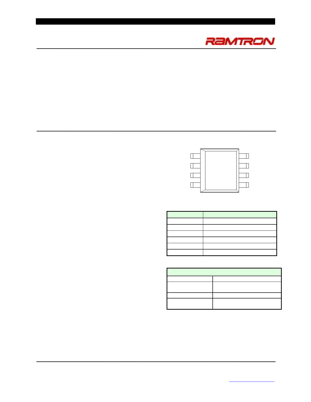
Pin Configuration
A0
A1
A2
VSS
1
2
3
4
8 VDD
7 WP
6 SCL
5 SDA
Pin Names
A0-A2
SDA
SCL
WP
VSS
VDD
Function
Device Select Address
Serial Data/Address
Serial Clock
Write Protect
Ground
Supply Voltage
Ordering Information
FM24W256-G
8-pin “Green”/RoHS SOIC
FM24W256-GTR
8-pin “Green”/RoHS SOIC, Tape
& Reel
FM24W256-EG*
8-pin “Green”/RoHS EIAJ SOIC
FM24W256-EGTR* 8-pin “Green”/RoHS EIAJ SOIC,
Tape & Reel
* Not Recommended for New Designs
This is a product that has fixed target specifications but are subject
to change pending characterization results.
Rev. 1.3
July 2011
Ramtron International Corporation
1850 Ramtron Drive, Colorado Springs, CO 80921
(800) 545-FRAM, (719) 481-7000
http://www.ramtron.com
Page 1 of 13
Datasheet pdf - http://www.DataSheet4U.net/
1 page 
www.DataSheet.co.kr
Slave ID
Device Select
1 0 1 0 A2 A1 A0 R/W
765 4 3 2 1
0
Figure 4. Slave Address
Addressing Overview
After the FM24W256 (as receiver) acknowledges the
slave address, the master can place the memory
address on the bus for a write operation. The address
requires two bytes. The first is the MSB. Since the
device uses only 15 address bits, the value of the
upper bit is “don’t care”. Following the MSB is the
LSB with the remaining eight address bits. The
address value is latched internally. Each access
causes the latched address value to be incremented
automatically. The current address is the value that is
held in the latch -- either a newly written value or the
address following the last access. The current address
will be held for as long as power remains or until a
new value is written. Reads always use the current
address. A random read address can be loaded by
beginning a write operation as explained below.
After transmission of each data byte, just prior to the
acknowledge, the FM24W256 increments the internal
address latch. This allows the next sequential byte to
be accessed with no additional addressing. After the
last address (7FFFh) is reached, the address latch will
roll over to 0000h. There is no limit to the number of
bytes that can be accessed with a single read or write
operation.
Data Transfer
After the address information has been transmitted,
data transfer between the bus master and the
FM24W256 can begin. For a read operation the
FM24W256 will place 8 data bits on the bus then
wait for an acknowledge from the master. If the
acknowledge occurs, the FM24W256 will transfer the
next sequential byte. If the acknowledge is not sent,
the FM24W256 will end the read operation. For a
write operation, the FM24W256 will accept 8 data
bits from the master then send an acknowledge. All
data transfer occurs MSB (most significant bit) first.
FM24W256 - 256Kb Wide Voltage I2C F-RAM
Memory Operation
The FM24W256 is designed to operate in a manner
very similar to other 2-wire interface memory
products. The major differences result from the
higher performance write capability of F-RAM
technology. These improvements result in some
differences between the FM24W256 and a similar
configuration EEPROM during writes. The
complete operation for both writes and reads is
explained below.
Write Operation
All writes begin with a slave address, then a
memory address. The bus master indicates a write
operation by setting the LSB of the slave address to
a 0. After addressing, the bus master sends each byte
of data to the memory and the memory generates an
acknowledge condition. Any number of sequential
bytes may be written. If the end of the address range
is reached internally, the address counter will wrap
from 7FFFh to 0000h.
Unlike other nonvolatile memory technologies,
there is no effective write delay with F-RAM. Since
the read and write access times of the underlying
memory are the same, the user experiences no delay
through the bus. The entire memory cycle occurs in
less time than a single bus clock. Therefore, any
operation including read or write can occur
immediately following a write. Acknowledge
polling, a technique used with EEPROMs to
determine if a write is complete is unnecessary and
will always return a ready condition.
Internally, an actual memory write occurs after the
8th data bit is transferred. It will be complete before
the acknowledge is sent. Therefore, if the user
desires to abort a write without altering the memory
contents, this should be done using start or stop
condition prior to the 8th data bit. The FM24W256
uses no page buffering.
The memory array can be write protected using the
WP pin. Setting the WP pin to a high condition
(VDD) will write-protect all addresses. The
FM24W256 will not acknowledge data bytes that
are written to protected addresses. In addition, the
address counter will not increment if writes are
attempted to these addresses. Setting WP to a low
state (VSS) will deactivate this feature. WP is pulled
down internally.
Figures 5 and 6 below illustrate a single-byte and
multiple-byte write cycles.
Rev. 1.3
July 2011
Page 5 of 13
Datasheet pdf - http://www.DataSheet4U.net/
5 Page 
www.DataSheet.co.kr
FM24W256 - 256Kb Wide Voltage I2C F-RAM
Mechanical Drawing
8-pin SOIC (JEDEC Standard MS-012 variation AA)
Recommended PCB Footprint
Pin 1
4.90 ±0.10
3.90 ±0.10 6.00 ±0.20
1.35
1.75
2.00
1.27
0.25
0.50
7.70
3.70
0.65
0.19
45 0.25
1.27 0.10
0.33 0.25
0.51
0.10 mm
0-8
0.40
1.27
Refer to JEDEC MS-012 for complete dimensions and notes.
All dimensions in millimeters.
SOIC Package Marking Scheme
XXXXXXX-P
RLLLLLLL
RICYYWW
Legend:
XXXXXX= part number, P= package type (G=SOIC, EG=EIAJ SOIC)
R=rev code, LLLLLLL= lot code
RIC=Ramtron Int’l Corp, YY=year, WW=work week
Example: FM24W256, “Green” SOIC package, Year 2010, Work Week 37
FM24W256-G
A00002G1
RIC1037
Rev. 1.3
July 2011
Page 11 of 13
Datasheet pdf - http://www.DataSheet4U.net/
11 Page | ||
| Páginas | Total 13 Páginas | |
| PDF Descargar | [ Datasheet FM24W256.PDF ] | |
Hoja de datos destacado
| Número de pieza | Descripción | Fabricantes |
| FM24W256 | 256-Kbit (32 K x 8) Serial (I2C) F-RAM | Cypress Semiconductor |
| FM24W256 | 256Kb Wide Voltage Serial F-RAM | Ramtron |
| Número de pieza | Descripción | Fabricantes |
| SLA6805M | High Voltage 3 phase Motor Driver IC. |
Sanken |
| SDC1742 | 12- and 14-Bit Hybrid Synchro / Resolver-to-Digital Converters. |
Analog Devices |
|
DataSheet.es es una pagina web que funciona como un repositorio de manuales o hoja de datos de muchos de los productos más populares, |
| DataSheet.es | 2020 | Privacy Policy | Contacto | Buscar |