|
|
|
PDF MAX13448E Data sheet ( Hoja de datos )
| Número de pieza | MAX13448E | |
| Descripción | 80V Fault-Protected Full-Duplex RS-485 Transceiver | |
| Fabricantes | Maxim Integrated Products | |
| Logotipo | ||
Hay una vista previa y un enlace de descarga de MAX13448E (archivo pdf) en la parte inferior de esta página. Total 14 Páginas | ||
|
No Preview Available !
www.DataSheet.co.kr
19-4098; Rev 0; 5/08
±80V Fault-Protected Full-Duplex
RS-485 Transceiver
General Description
The MAX13448E full-duplex RS-485 transceiver fea-
tures inputs and outputs fault protected up to ±80V
(with respect to ground). The device operates from a
+3.0V to +5.5V supply and features true fail-safe cir-
cuitry, guaranteeing a logic-high receiver output when
the receiver inputs are open or shorted. This enables all
receiver outputs on a terminated bus to output logic-
high when all transmitters are disabled.
The MAX13448E features a slew-rate limited driver that
minimizes EMI and reduces reflections caused by
improperly terminated cables, allowing error-free data
transmission at data rates up to 500kbps with a +5V
supply, and 250kbps with a +3.3V supply.
The MAX13448E includes a hot-swap capability to elimi-
nate false transitions on the bus during power-up or hot
insertion. The driver and receiver feature active-high and
active-low enables, respectively, that can be connected
together externally to serve as a direction control.
The MAX13448E features an 1/8-unit load receiver input
impedance, allowing up to 256 transceivers on the bus.
All driver outputs are protected to ±8kV ESD using the
Human Body Model. The MAX13448E is available in a
14-pin SO package and operates over the extended
-40°C to +85°C temperature range.
Applications
Industrial Control Systems
HVAC Control systems
Utility Meters
Motor Driver Control Systems
Features
o ±80V Fault Protection on the RS-485 I/O Ports
o True Fail-Safe Receiver
o Hot-Swap Input Structure on DE
o ESD Protection on the RS-485 I/O Ports
±8kV Human Body Model
o Slew-Rate Limiting Facilitates Error-Free Data
Transmission
o 1/8-Unit Load Allows Up to 256 Transceivers on
the Bus
o -7V to +12V Common-Mode Input Voltage Range
o +3.0V to +5.5V Operating Supply Voltage
o Available in 14-Pin SO Package
Ordering Information
PART
TEMP RANGE
MAX13448EESD+ -40°C to +85°C
+Denotes a lead-free package.
PIN-PACKAGE
14 SO
Pin Configuration appears at end of data sheet.
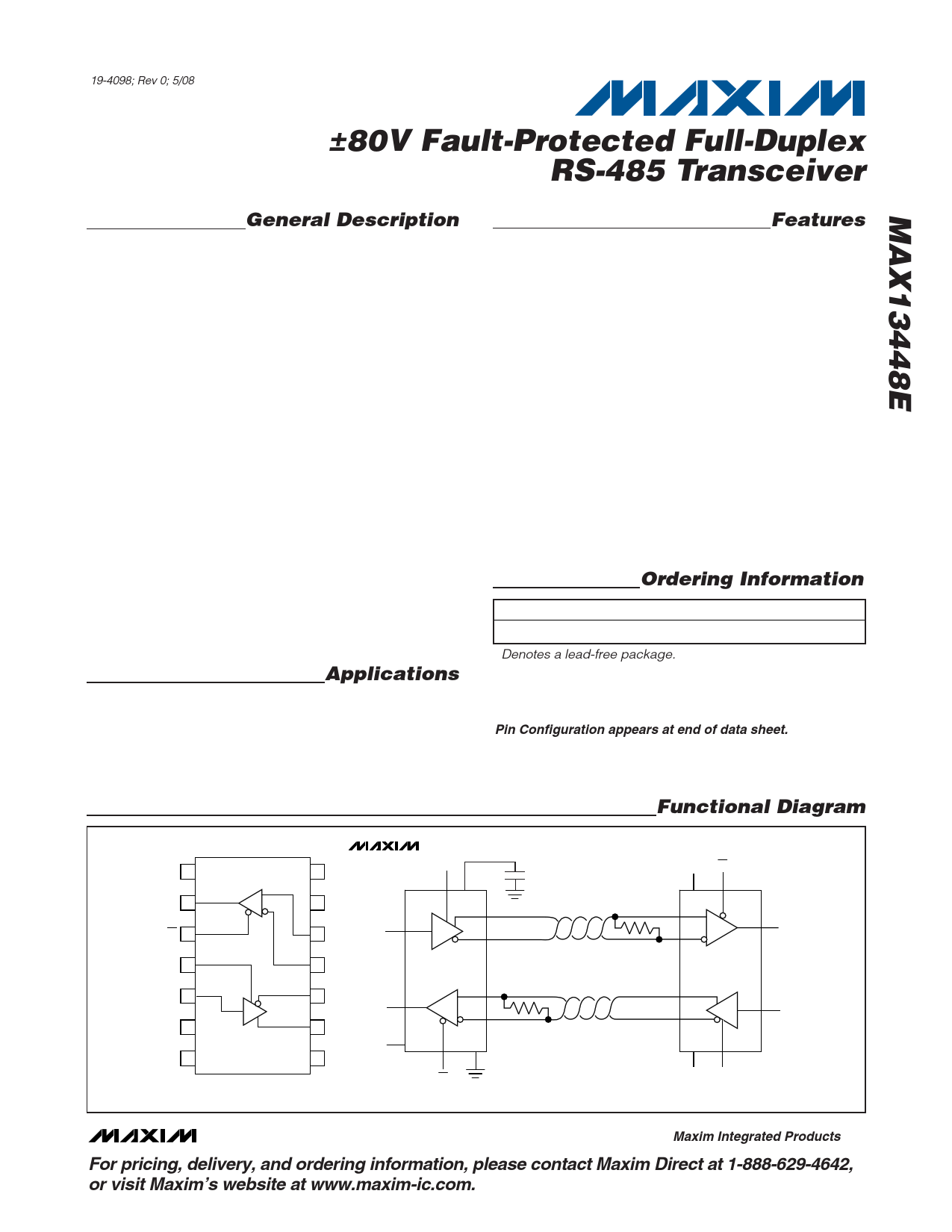
Functional Diagram
N.C. 1 +
RO 2
RE 3
DE 4
DI 5
GND 6
GND 7
R
D
SO
MAX13448E
14 VCC
13 N.C.
12 A
5
DI
11 B
10 Z
9Y
8 N.C.
2
RO
1, 8,
13
N.C.
DE VCC
4 14
9
D 10
12
R 11
3 6, 7
RE GND
1μF
Y
Z
A
Rt
B
VCC RE
Rt R
RO
D DI
GND DE
________________________________________________________________ Maxim Integrated Products 1
For pricing, delivery, and ordering information, please contact Maxim Direct at 1-888-629-4642,
or visit Maxim’s website at www.maxim-ic.com.
Datasheet pdf - http://www.DataSheet4U.net/
1 page 
www.DataSheet.co.kr
±80V Fault-Protected Full-Duplex
RS-485 Transceiver
SWITCHING CHARACTERISTICS (VCC = +5V ±10%) (continued)
(TA = TMIN to TMAX, unless otherwise noted. Typical values are at VCC = +5V and TA = +25°C.)
PARAMETER
Driver Enable Time to Output High
Driver Disable Time from
Output High
SYMBOL
CONDITION
tDZH RL = 500Ω, CL = 50pF, Figure 4
tDHZ RL = 500Ω, CL = 50pF, Figure 4
MIN TYP MAX UNITS
1500
ns
1000
ns
Driver Enable Time from
Shutdown to Output High
tDZH(SHDN) RL = 500Ω, CL = 50pF, Figure 4
Driver Enable Time to Output Low
tDZL RL = 500Ω, CL = 50pF, Figure 5
Driver Disable Time from
Output Low
tDLZ RL = 500Ω, CL = 50pF, Figure 5
8
1000
2
µs
ns
µs
Driver Enable Time from
Shutdown to Output Low
Driver Time to Shutdown
RECEIVER
tDZL(SHDN) RL = 500Ω, CL = 50pF, Figure 5
tSHDN RL = 500Ω, CL = 50pF
8 µs
12 µs
Receiver Propagation Delay
Receiver Output Skew
tRPLH,
tRPHL
tRSKEW
CL = 20pF, VID = 2V, VCM = 0V,
Figure 6
CL = 20pF, tRSKEW = [tRPLH - tRPHL],
Figure 6
2000
200
ns
ns
Receiver Enable Time to
Output High
tRZH RL = 1kΩ, CL = 20pF, Figure 7
1000
ns
Receiver Disable Time from
Output High
tRHZ RL = 1kΩ, CL = 20pF, Figure 7
150 ns
Receiver Wake Time from
Shutdown
tRWAKE RL = 1kΩ, CL = 20pF, Figure 7
8 µs
Receiver Enable Time to
Output Low
tRZL RL = 1kΩ, CL = 20pF, Figure 7
1000
ns
Receiver Disable Time from
Output Low
Receiver Time to Shutdown
tRLZ
tSHDN
RL = 1kΩ, CL = 20pF, Figure 7
RL = 500Ω, CL = 50pF
150 ns
150 ns
Note 2: Parameters are 100% production tested at TA = +25°C, unless otherwise noted. Limits over temperature are guaranteed by
design.
Note 3: All currents into the device are positive. All currents out of the device are negative. All voltages are referenced to device
ground, unless otherwise noted.
Note 4: ΔVOD and ΔVOC are the changes in VOD and VOC, respectively, when the DI input changes state.
Note 5: The short-circuit output current applies to peak current just prior to foldback current limiting. The short-circuit foldback output
current applies during current limiting to allow a recover from bus contention.
_______________________________________________________________________________________ 5
Datasheet pdf - http://www.DataSheet4U.net/
5 Page 
www.DataSheet.co.kr
±80V Fault-Protected Full-Duplex
RS-485 Transceiver
Detailed Description
The MAX13448E ±80V fault-protected RS-485/RS-422
transceiver contains one driver and one receiver. This
device features fail-safe circuitry, guaranteeing a logic-
high receiver output when the receiver inputs are open
or shorted, or when they are connected to a terminated
transmission line with all drivers disabled. The device
has a hot-swap input structure that prevents distur-
bances on the differential signal lines when a circuit
board is plugged into a hot backplane. All receiver
inputs and driver outputs are protected to ±8kV ESD
using the Human Body Model. The MAX13448E
features a reduced slew-rate driver that minimizes
EMI and reduces reflections caused by improperly
terminated cables, allowing error-free data transmis-
sion up to 500kbps.
Driver
The driver accepts a single-ended, logic-level input
(DI) and converts it to a differential, RS-485/RS-422
level output (A and B). Deasserting the driver enable
places the driver outputs (A and B) into a high-imped-
ance state.
Receiver
The receiver accepts a differential, RS-485/RS-422
level input (A and B), and translates it to a single-
ended, logic-level output (RO). Deasserting the receiv-
er enable places the receiver outputs (RO) into a
high-impedance state (see Table 1).
Low-Power Shutdown
Low-power shutdown is initiated by bringing DE low
and RE high. In shutdown, the device draws a maxi-
mum of 100µA of supply current.
The device is guaranteed to not enter shutdown if DE is
low and RE is high for 1µs. If the inputs are in this state
for at least 1ms, the device is guaranteed to enter shut-
down. In the shutdown state, the driver outputs (A and
B) as well as the receiver output (RO) are in a high-
impedance state.
±80V Fault Protection
In certain applications, such as industrial control, driver
outputs and receiver inputs of an RS-485 device some-
times experience common-mode voltages in excess of
the -7V to +12V range specified in the EIA/TIA-485
standard. In these applications, ordinary RS-485
devices (typical absolute maximum ratings of -8V to
+12.5V) may experience damage without the addition
of external protection devices.
Table 1. Function Table
TRANSMITTING
INPUT
RE DE DI
OUTPUT
ZY
X10
1
0
X11
0
1
00X
High
High
Impedance Impedance
1 0 X High Impedance (Shutdown)
RECEIVING
INPUT
RE DE A - B
OUTPUT
RO
0 X -50mV
1
0 X -200mV
0
11X
Disabled
1 0 X High Impedance (Shutdown)
X = Don’t care; shutdown mode, driver, and receiver outputs are
high impedance.
To reduce system complexity and the need for external
protection, the driver outputs and receiver inputs of the
MAX13448E withstand voltage faults of up to ±80V with
respect to ground without damage (see the Absolute
Maximum Ratings section, Note 1). Protection is guar-
anteed regardless of whether the device is active, in
shutdown, or without power. Certain parasitic effects
present while driving an unterminated cable may cause
the voltage seen at driver outputs to exceed the
absolute maximum limit, while the DI input is switched
during a ±80V fault on the A or B input. Therefore, a
termination resistor is recommend in order to maximize
the overvoltage fault protection while the DI input is
being switched. If the DI input does not change state
while the fault voltage is present, the MAX13448E will
withstand up the ±80V on the RS-485 inputs, regard-
less of the presence of a termination resistor. While the
MAX13448E is not damaged by up to ±80V common-
mode voltages, the RO, Y, and Z outputs will be in an
indeterminate state if the common-mode voltage
exceeds -7V to +12V.
True Fail-Safe
The MAX13448E guarantees a logic-high receiver out-
put when the receiver inputs are shorted or open, or
when they are connected to a terminated transmission
line with all drivers disabled. This is done by setting the
______________________________________________________________________________________ 11
Datasheet pdf - http://www.DataSheet4U.net/
11 Page | ||
| Páginas | Total 14 Páginas | |
| PDF Descargar | [ Datasheet MAX13448E.PDF ] | |
Hoja de datos destacado
| Número de pieza | Descripción | Fabricantes |
| MAX13448E | 80V Fault-Protected Full-Duplex RS-485 Transceiver | Maxim Integrated Products |
| Número de pieza | Descripción | Fabricantes |
| SLA6805M | High Voltage 3 phase Motor Driver IC. |
Sanken |
| SDC1742 | 12- and 14-Bit Hybrid Synchro / Resolver-to-Digital Converters. |
Analog Devices |
|
DataSheet.es es una pagina web que funciona como un repositorio de manuales o hoja de datos de muchos de los productos más populares, |
| DataSheet.es | 2020 | Privacy Policy | Contacto | Buscar |