|
|
|
PDF OV9665 Data sheet ( Hoja de datos )
| Número de pieza | OV9665 | |
| Descripción | Color CMOS SXGA CameraChip Sensor | |
| Fabricantes | OmniVision | |
| Logotipo | ||
Hay una vista previa y un enlace de descarga de OV9665 (archivo pdf) en la parte inferior de esta página. Total 30 Páginas | ||
|
No Preview Available !
www.DataSheet.co.kr
Omni ision
®
Advanced Information
Datasheet
OV9665 Color CMOS SXGA (1.3 MegaPixel) CAMERACHIPTM Sensor
with OmniPixel2TM Technology
General Description
The OV9665 CAMERACHIP™ image sensor is a low
voltage CMOS device that provides the full functionality of
a single-chip SXGA (1280x1024) camera and image
processor in a small footprint package. The OV9665
provides full-frame, sub-sampled, scaled or windowed
8-bit/10-bit images in a wide range of formats, controlled
through the Serial Camera Control Bus (SCCB) interface.
This product has an image array capable of operating at
up to 15 frames per second (fps) in SXGA resolution with
complete user control over image quality, formatting and
output data transfer. All required image processing
functions, including exposure control, gamma, white
balance, color saturation, hue control, defect pixel
canceling, noise canceling, and more, are also
programmable through the SCCB interface. In addition,
OmniVision sensors use proprietary sensor technology to
improve image quality by reducing or eliminating common
lighting/electrical sources of image contamination, such
as fixed pattern noise, smearing, etc., to produce a clean,
fully stable color image.
Note: The OV9665 uses a lead-free
Pb package.
Features
• High sensitivity for low-light operation
• Low operating voltage for embedded portable
applications
• Standard SCCB interface
• Supports image sizes: SXGA, VGA, CIF, scaled
down and windowed outputs with Raw RGB,
RGB565/555/444, YUV (4:2:2) and YCbCr (4:2:2)
formats
• VarioPixel® method for sub-sampling
• Automatic image control functions including
Automatic Exposure Control (AEC), Automatic Gain
Control (AGC), Automatic White Balance (AWB), and
Automatic Black-Level Calibration (ABLC)
• Image quality controls including color saturation,
hue, gamma, sharpness (edge enhancement), lens
correction, defect pixel canceling, noise canceling,
and 50/60 Hz luminance detection
Ordering Information
Product
OV09665-VL9A (Color, lead-free)
Package
26-pin CSP2
Applications
• Cellular and Picture Phones
• Toys
• PC Multimedia
• Digital Still Cameras
Key Specifications
Active Array Size 1304 x 1036
Power Supply
Analog 2.45 to 3.0VDC
I/O 1.71V to 3.0V
Power
Active 80 mW typical (15fps)
Requirements
Standby 15 µA typical
Temperature
Operation -30°C to 70°C
Range
Stable Image 0°C to 50°C
• YUV/YCbCr 4:2:2
Output Formats (8-bit) • RGB565/555/444
• Raw RGB Data
Lens Size 1/5.5"
Chief Ray Angle 25° non-linear
Maximum
Image
Transfer Rate
SXGA 15 fps
VGA and down
scaling
30
fps
Sensitivity 450 mV/(Lux • sec)
S/N Ratio 40 dB
Dynamic Range 55 dB
Scan Mode Progressive
Maximum Exposure Interval 1052 x tROW
Gamma Correction Programmable
Pixel Size 2.0 µm x 2.0 µm
Dark Current 3 mV/sec @ 60°C
Well Capacity 13 Ke
Fixed Pattern Noise 1% of VPEAK-TO-PEAK
Image Area 2608 µm x 2072 µm
Package Dimensions 4485 µm x 4985 µm
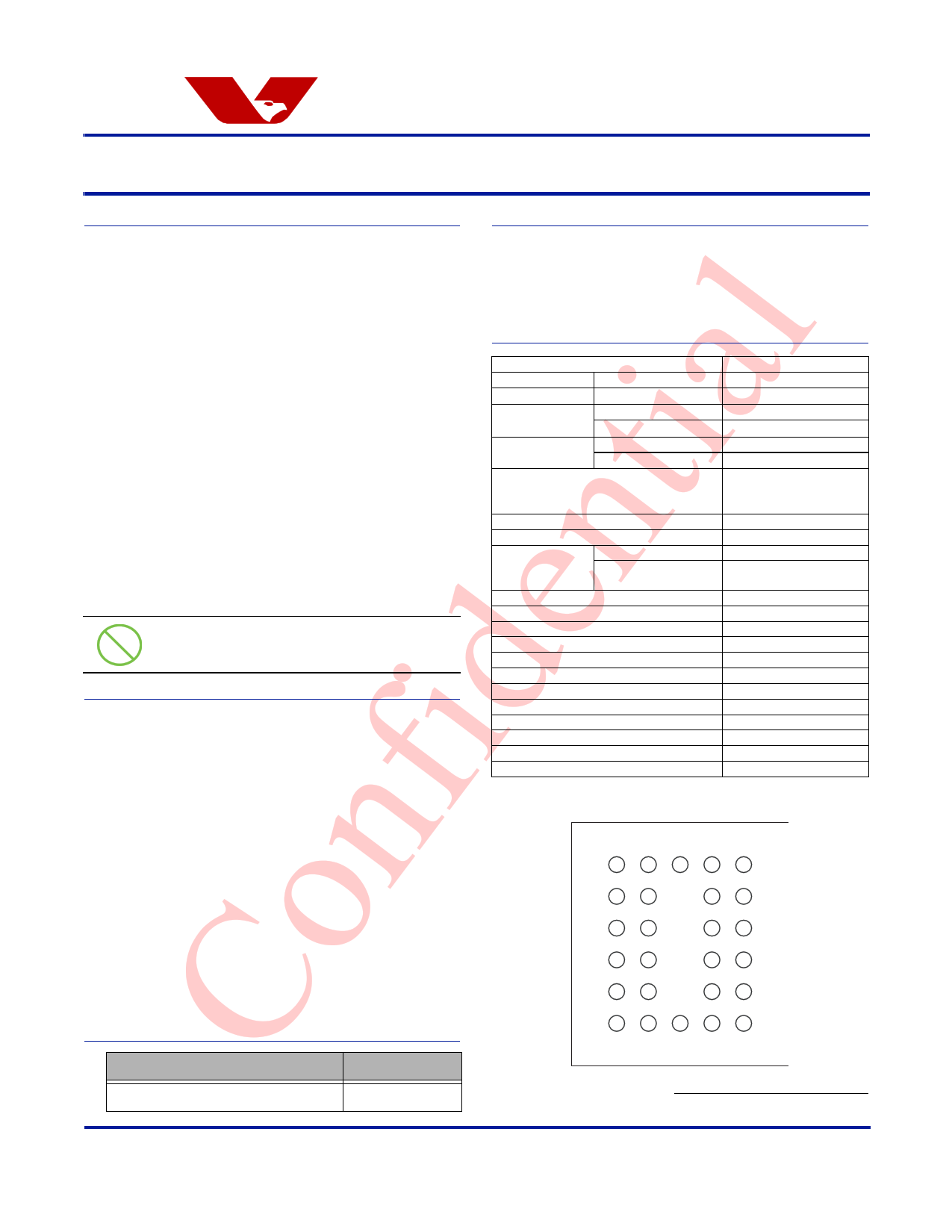
Figure 1 OV9665 Pin Diagram (Top View)1
A1 A2 A3 A4 A5
VREFH VREFN D8 D6 D7
B1 B2
AGND AVDD
B4 B5
D4 D5
C1 C2
C4 C5
PWDN RESETB
D2
OV9665
D1 D2
D4
D3
D5
SIO_C SIO_D
D0/STROBE D1
E1
XVCLK
E2
D9
E4 E5
VREFD VSYNC
F1 F2 F3 F4
DOGND DOVDD VREFD PCLK
F5
HREF
9665CSP_DS_001
1 OV9665 pin diagram © 2008 OmniVision Technologies, Inc.
© 2008 OmniVision Technologies, Inc.
Version 1.1, October 10, 2007
VarioPixel, OmniVision, and the OmniVision logo are registered trademarks of OmniVision Technologies, Inc.
CameraChip and OmniPixel2 are trademarks of OmniVision Technologies, Inc.
These specifications are subject to change without notice.
Datasheet pdf - http://www.DataSheet4U.net/
1 page 
www.DataSheet.co.kr
Omni ision
Electrical Characteristics
Electrical Characteristics
Table 2
Absolute Maximum Ratings
Ambient Storage Temperature
Supply Voltages (with respect to Ground)
All Input/Output Voltages (with respect to Ground)
Lead-free Temperature, Surface-mount process
VDD-A
VDD-IO
-40ºC to +95ºC
4.5 V
4.5 V
-0.3V to VDD-IO+0.5V
245ºC
NOTE: Exceeding the Absolute Maximum ratings shown above invalidates all AC and DC electrical specifications and may
result in permanent device damage.
Table 3
DC Characteristics (-30°C < TA < 70°C)
Symbol
Parameter
Condition
Min
Typ
Max
VDD-A
DC supply voltage – analog
–
2.45 2.8
3.0
VDD-IO
IDDA
DC supply voltage – I/O
Active (operating) current
–
See Note a
1.71
1.8
17 + 18b
3.0
50
IDDS-SCCB
IDDS-PWDN
Standby current
Standby current
See Note c
12
15 30
VIH Input voltage HIGH
CMOS
0.7 x VDD-IO
VIL Input voltage LOW
0.3 x VDD-IO
VOH Output voltage HIGH
CMOS
0.9 x VDD-IO
VOL Output voltage LOW
0.1 x VDD-IO
a. At 25°C, VDD-A = 2.8V, VDD-IO = 1.8V
IDDA = ∑{IDD-A + IDD-IO}, fCLK = 24MHz at 15 fps YCbCr output with typical loading
b. IDD-IO = 17mA, IDD-A = 18mA, with typical loading
c. At 25°C, VDD-A = 2.8V, VDD-IO = 1.8V
IDDS-SCCB refers to a SCCB-initiated Standby, while IDDS-PWDN refers to a PWDN pin-initiated Standby
Unit
V
V
mA
mA
µA
V
V
V
V
Version 1.1, October 10, 2007
Proprietary to OmniVision Technologies, Inc.
5
Datasheet pdf - http://www.DataSheet4U.net/
5 Page 
www.DataSheet.co.kr
Omni ision
Register Table
Register Table
Table 5 provides a list and description of the Device Control registers contained in the OV9665. For all register Enable/Disable
bits, ENABLE = 1 and DISABLE = 0. The device slave addresses are 0x60 for write and 0x61 for read.
Note: Reserved registers or register bits may be non-functional, special
function or sensitive to the sensor. Please refer to OmniVision’s
recommended register settings.
Table 5
Address
(Hex)
00
01
02
03
04
05
Device Control Register List (Sheet 1 of 16)
Register
Name
GAIN
Default
(Hex) R/W
Description
AGC Gain Control
Bit[7:0]: Gain setting
00 RW
• Range: 1x to 32x
Gain = (Bit[7]+1) x (Bit[6]+1) x (Bit[5]+1) x (Bit[4]+1) x (1+Bit[3:0])/16)
BLUE
RED
COM1
REG04
REG05
NOTE: Set COM8[2] = 0 to disable AGC.
40 RW Blue Gain Control
40 RW Blue Gain Control
Common Control 1
Bit[7:6]: Dummy frame control - effective when register bit
COM6[3] = 1 (0x0F) (night mode enable)
03 RW
Bit[5:4]:
00: Not used
01: Allow 1 dummy frame
10: Allow 3 dummy frames
11: Allow 7 dummy frames
Reserved
Bit[3:2]: Vertical window end line control 2 LSBs (see register
VEND for 8 MSBs)
Bit[1:0]: Vertical window start line control 2 LSBs (see register
VSTRT for 8 MSBs)
Register 04
28 RW
Bit[7]:
Bit[6]:
Horizontal mirror (effective when register bit
REG33[3] = 1 (0x33)
Vertical flip
Bit[5:2]: Reserved
Bit[1:0]: AEC low 2 LSBs – AEC[1:0] (see register AEC for
AEC[9:2] and register REG45[5:0] for AEC[15:10])
Register 05
00 RW
Bit[7:3]:
Bit[2:0]:
Reserved
UV adjust slope[5:3] between gain threshold 1 and gain
threshold 2. For others, refer to registers COM1[5:4]
(0x03) and REG60[2:0] (0x60).
Version 1.1, October 10, 2007
Proprietary to OmniVision Technologies, Inc.
11
Datasheet pdf - http://www.DataSheet4U.net/
11 Page | ||
| Páginas | Total 30 Páginas | |
| PDF Descargar | [ Datasheet OV9665.PDF ] | |
Hoja de datos destacado
| Número de pieza | Descripción | Fabricantes |
| OV9665 | Color CMOS SXGA CameraChip Sensor | OmniVision |
| Número de pieza | Descripción | Fabricantes |
| SLA6805M | High Voltage 3 phase Motor Driver IC. |
Sanken |
| SDC1742 | 12- and 14-Bit Hybrid Synchro / Resolver-to-Digital Converters. |
Analog Devices |
|
DataSheet.es es una pagina web que funciona como un repositorio de manuales o hoja de datos de muchos de los productos más populares, |
| DataSheet.es | 2020 | Privacy Policy | Contacto | Buscar |