|
|
|
PDF ADP5042 Data sheet ( Hoja de datos )
| Número de pieza | ADP5042 | |
| Descripción | Micro PMU | |
| Fabricantes | Analog Devices | |
| Logotipo | ||
Hay una vista previa y un enlace de descarga de ADP5042 (archivo pdf) en la parte inferior de esta página. Total 30 Páginas | ||
|
No Preview Available !
www.DataSheet4U.net
Micro PMU with 0.8 A Buck, Two 300 mA LDOs
Supervisory, Watchdog and Manual Reset
ADP5042
FEATURES
Input voltage range: 2.3 V to 5.5 V
One 0.8 A buck regulator
Two 300 mA LDOs
20-lead, 4 mm × 4 mm LFCSP package
Initial regulator accuracy: ±1%
Overcurrent and thermal protection
Soft start
Undervoltage lockout
Open drain processor reset with threshold monitoring
±1.5% threshold accuracy over the full temperate range
Guaranteed reset output valid to VCC = 1 V
Dual watchdog for secure systems
Watchdog 1 controls reset
Watchdog 2 controls reset and regulators power cycle
Buck key specifications
Current mode topology for excellent transient response
3 MHz operating frequency
Uses tiny multilayer inductors and capacitors
Mode pin selects forced PWM or auto PFM/PSM modes
100% duty cycle low dropout mode
LDOs key specifications
Low VIN from 1.7 V to 5.5 V
Stable with1 μF ceramic output capacitors
High PSRR, 60 dB PSRR up to 1 kHz/10 kHz
Low output noise
110 μV rms typical output noise at VOUT = 2.8 V
Low dropout voltage: 150 mV at 300 mA load
−40°C to +125°C junction temperature range
GENERAL DESCRIPTION
The ADP5042 combines one high performance buck regulator
and two low dropout regulators (LDO) in a small 20-lead
LFCSP to meet demanding performance and board space
requirements.
The high switching frequency of the buck regulator enables
use of tiny multilayer external components and minimizes the
board space.
The MODE pin selects the buck mode of operation. When set
to logic high, the buck regulators operate in forced PWM mode.
When the MODE pin is set to logic low, the buck regulators
operate in PWM mode when the load is around the nominal
value. When the load current falls below a predefined threshold
the regulator operates in power save mode (PSM) improving
the light-load efficiency.
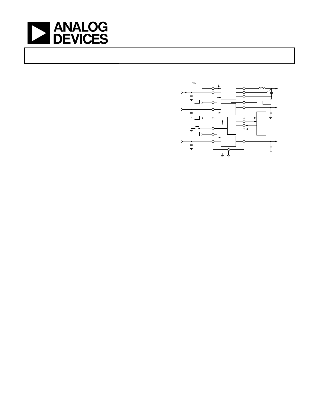
HIGH LEVEL BLOCK DIAGRAM
RFILT = 30Ω
VIN1 = 2.3V
TO 5.5V
C5
4.7µF
AVIN
VIN1
ON
OFF
EN1
VIN2 = 1.7V
TO 5.5V
C1
1µF
VIN2
ON
OFF
EN2
AVIN
BUCK
EN_BK
LDO1
(DIGITAL)
EN_LDO1
AVIN
VIN3 = 1.7V
TO 5.5V
C3
1µF
ON
OFF
MR
EN3
VIN3
EN_LDO2
LDO2
(ANALOG)
AGND
SW
VOUT1
PGND
L1
1µH
VOUT1 AT
C6 800mA
10µF
MODE
VOUT2
WSTAT
nRSTO
FPWM
PSM/PWM
VOUT2 AT
300mA
C2
1µF
WDI1
WDI2
VOUT3
VOUT3 AT
300mA
C4
1µF
Figure 1.
The low quiescent current, low dropout voltage, and wide input
voltage range of the ADP5042 LDOs extend the battery life of
portable devices. The two LDOs maintain power supply
rejection greater than 60 dB for frequencies as high as 10 kHz
while operating with a low headroom voltage.
Each regulator is activated by a high level on the respective
enable pin. The ADP5042 is available with factory programmable
default output voltages and can be set to a wide range of options.
The ADP5042 contains supervisory circuits that monitor
power supply voltage levels and code execution integrity in
microprocessor-based systems. They also provide power-on
reset signals. An on-chip dual watchdog timer can reset the
microprocessor or power cycle the system (Watchdog 2) if it
fails to strobe within a preset timeout period.
Rev. 0
Information furnished by Analog Devices is believed to be accurate and reliable. However, no
responsibility is assumed by Analog Devices for its use, nor for any infringements of patents or other
rights of third parties that may result from its use. Specifications subject to change without notice. No
license is granted by implication or otherwise under any patent or patent rights of Analog Devices.
Trademarksandregisteredtrademarksarethepropertyoftheirrespectiveowners.
One Technology Way, P.O. Box 9106, Norwood, MA 02062-9106, U.S.A.
Tel: 781.329.4700
www.analog.com
Fax: 781.461.3113
©2010 Analog Devices, Inc. All rights reserved.
1 page 
ADP5042
BUCK SPECIFICATIONS
AVIN, VIN1 = 3.6 V, VOUT1 = 1.8 V, TJ= −40°C to +125°C for minimum/maximum specifications, L = 1 µH, COUT = 10 µF, and TA = 25°C
for typical specifications, unless otherwise noted.1
Table 3.
Parameter
INPUT CHARACTERISTICS
Input Voltage Range (VIN1)
OUTPUT CHARACTERISTICS
Output Voltage Accuracy
PWM TO POWER SAVE MODE CURRENT THRESHOLD
INPUT CURRENT CHARACTERISTICS
DC Operating Current
Shutdown Current
SW CHARACTERISTICS
SW On Resistance
Current Limit
ACTIVE PULL-DOWN
OSCILLATOR FREQUENCY
START-UP TIME
Test Conditions/Comments
PWM mode, TA= 25 °C , ILOAD = 100 mA
PWM mode
VIN1 = 2.3 V to 5.5 V, PWM mode,
ILOAD = 1 to 800 mA
ILOAD = 0 mA, device not switching
ENx = 0 V, TA = TJ = −40°C to +125°C
PFET
PFET, AVIN = VIN1 = 5 V
NFET
NFET, AVIN = VIN1 = 5 V
PFET switch peak current limit
EN1 = 0 V
Min
2.3
−1
−2
−3
1100
2.5
Typ
100
21
0.2
180
140
170
150
1360
75
3.0
250
Max
5.5
+1
+2
+3
35
1.0
240
190
235
210
1600
3.5
Unit
V
%
%
%
mA
μA
μA
mΩ
mΩ
mΩ
mΩ
mA
Ω
MHz
μs
1 All limits at temperature extremes are guaranteed via correlation using standard statistical quality control (SQC).
LDO1, LDO2 SPECIFICATIONS
AVIN = 3.6 V, VIN2, VIN3 = (VOUT3 + 0.2 V) or 2.3 V, whichever is greater; AVIN, VIN1 ≥ VIN2, VIN3; IOUT = 10 mA; CIN = COUT = 1 µF;
TA = 25°C, unless otherwise noted.
Table 4.
Parameter
INPUT VOLTAGE RANGE
OPERATING SUPPLY CURRENT (per
LDO)
Symbol
VIN2, VIN3
IGND
FIXED OUTPUT VOLTAGE ACCURACY VOUT2, VOUT3
REGULATION
Line Regulation
∆VOUT2/∆VIN2
∆VOUT3/∆VIN3
Conditions
TJ = −40°C to +125°C
IOUT = 0 µA, VOUT = 3.3 V
IOUT = 0 µA, VOUT = 3.3 V, TJ = −40°C to +125°C
IOUT = 10 mA
IOUT = 10 mA, TJ = −40°C to +125°C
IOUT = 200 mA
IOUT = 200 mA, TJ = −40°C to +125°C
IOUT = 10 mA
100 µA < IOUT < 300 mA
VIN2, VIN3 = (VOUT2, VOUT3 + 0.5 V) to 5.5 V
100 µA < IOUT < 300 mA
VIN2, VIN3 = (VOUT2, VOUT3 + 0.5 V) to 5.5 V
TJ = −40°C to +125°C
Min
1.7
−1
−2
−3
Typ
15
67
100
VIN2, VIN3 = (VOUT2, VOUT3 + 0.5 V) to 5.5 V
IOUT3 = 1 mA
TJ = −40°C to +125°C
−0.03
Max Unit
5.5 V
µA
50 µA
µA
105 µA
µA
245 µA
+1 %
+2 %
+3 %
+0.03 %/ V
Rev. 0 | Page 5 of 32
5 Page 
100
90
80 –40ºC
+25ºC
70 +85ºC
60
50
40
30
20
10
0
0.001
0.01
0.1
1
OUTPUT CURRENT (A)
Figure 15. Buck Efficiency vs. Load Current, Across Temperature, VOUT1 = 1.8 V,
PWM Mode
100
–40°C
90 +25°C
+85°C
80
70
60
50
40
30
20
10
0
0.0001
0.001
0.01
0.1
1
OUTPUT CURRENT (A)
Figure 16. Buck Efficiency vs. Load Current, Across Temperature, VOUT1 = 3.3 V,
Auto Mode
100
–40°C
90 +25°C
+85°C
80
70
60
50
40
30
20
10
0
0.0001
0.001
0.01
0.1
1
OUTPUT CURRENT (A)
Figure 17. Buck Efficiency vs. Load Current, Across Temperature, VOUT1 = 1.8 V,
Auto Mode
ADP5042
1.7
1.6
1.5
1.4
1.3
1.2
1.1
1.0
2.6 3.6 4.6 5.6
INPUT VOLTAGE (V)
Figure 18. Buck DC Current Capability vs. Input Voltage, VOUT1 = 1.8 V
3.10
–40°C
3.05
+25°C
3.00
2.95
+85°C
2.90
2.85
0
0.1 0.2 0.3 0.4 0.5 0.6 0.7 0.8
OUTPUT CURRENT (A)
Figure 19. Buck Switching Frequency vs. Output Current, Across Temperature,
VOUT1 = 1.8 V, PWM Mode
VOUT
1
ISW
2
SW
3
CH1 20.0mV/DIV
BW 20.0M
CH2 200mA/DIV 1MΩ BW 20.0M
CH3 2.0V/DIV 1MΩ BW 20.0M
A CH1
2.4mV
5.0µs/DIV
20.0MS/s
50.0ns/pt
Figure 20. Typical Waveforms, VOUT1 = 3.3 V, IOUT1 = 30 mA, Auto Mode
Rev. 0 | Page 11 of 32
11 Page | ||
| Páginas | Total 30 Páginas | |
| PDF Descargar | [ Datasheet ADP5042.PDF ] | |
Hoja de datos destacado
| Número de pieza | Descripción | Fabricantes |
| ADP5040 | Micro PMU | Analog Devices |
| ADP5041 | Micro PMU | Analog Devices |
| ADP5042 | Micro PMU | Analog Devices |
| ADP5043 | Micro PMU | Analog Devices |
| Número de pieza | Descripción | Fabricantes |
| SLA6805M | High Voltage 3 phase Motor Driver IC. |
Sanken |
| SDC1742 | 12- and 14-Bit Hybrid Synchro / Resolver-to-Digital Converters. |
Analog Devices |
|
DataSheet.es es una pagina web que funciona como un repositorio de manuales o hoja de datos de muchos de los productos más populares, |
| DataSheet.es | 2020 | Privacy Policy | Contacto | Buscar |