|
|
|
PDF ADP2126 Data sheet ( Hoja de datos )
| Número de pieza | ADP2126 | |
| Descripción | (ADP2126 / ADP2127) DC-to-DC Converters | |
| Fabricantes | Analog Devices | |
| Logotipo | ||
Hay una vista previa y un enlace de descarga de ADP2126 (archivo pdf) en la parte inferior de esta página. Total 20 Páginas | ||
|
No Preview Available !
www.DataSheet4U.net
Ultralow Profile, 500 mA, 6 MHz, Synchronous,
Step-Down, DC-to-DC Converters
ADP2126/ADP2127
FEATURES
1.20 V and 1.26 V fixed output voltage options
Clock signal enable
Logic signal enable also available on certain models
6 MHz operating frequency
Spread spectrum frequency modulation to reduce EMI
500 mA continuous output current
Input voltage: 2.1 V to 5.5 V
0.3 μA (typical) shutdown supply current
Pin-selectable power-saving mode
Compatible with tiny multilayer inductors
Internal synchronous rectifier
Internal compensation
Internal soft start
Output-to-ground short-circuit protection
Current-limit protection
Undervoltage lockout
Thermal shutdown protection
0.330 mm height (maximum), 6-ball BUMPED_CHIP (ADP2126)
0.200 mm height (maximum), 6-pad EWLP (ADP2127)
APPLICATIONS
Mobile phones
Digital still/video cameras
Digital audio
Portable equipment
Camera modules
Image stabilization systems
GENERAL DESCRIPTION
The ADP2126/ADP2127 are high frequency, step-down, dc-to-
dc converters optimized for portable applications in which board
area and battery life are critical constraints. The fixed 6 MHz
operating frequency enables the use of tiny ceramic inductors
and capacitors and the regulators use spread spectrum frequency
modulation to reduce EMI. Additionally, synchronous rectification
improves efficiency and results in fewer external components.
At high load currents, the ADP2126/ADP2127 use a voltage
regulating pulse-width modulation (PWM) mode that maintains
a constant frequency with excellent stability and transient response.
Light load operation is determined by the state of the MODE pin.
In forced PWM mode, the converter continues operating in PWM
for light loads. Under light load conditions in auto mode, the
ADP2126/ADP2127 automatically enter a power-saving mode,
which uses pulse frequency modulation (PFM) to reduce the
effective switching frequency, thus ensuring the longest battery
life in portable applications.
Rev. A
Information furnished by Analog Devices is believed to be accurate and reliable. However, no
responsibility is assumed by Analog Devices for its use, nor for any infringements of patents or other
rights of third parties that may result from its use. Specifications subject to change without notice. No
license is granted by implication or otherwise under any patent or patent rights of Analog Devices.
Trademarksandregisteredtrademarksarethepropertyoftheirrespectiveowners.
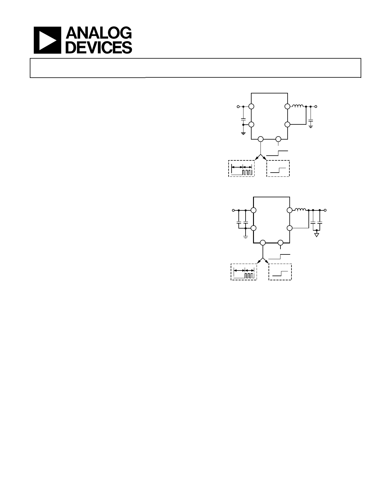
TYPICAL APPLICATION CIRCUITS
INPUT
VOLTAGE
2.1V TO 5.5V
CIN
2.2µF
ADP2126
L
1.0µH
A2 VIN
SW B1
C2 GND
FB C1
OUTPUT
VOLTAGE
1.20V OR 1.26V
COUT
2.2µF
EXTCLK MODE
B2 A1
PWM
AUTO
OFF ON
OR
ON *
OFF
*LOGIC HIGH ENABLE IS ONLY AVAILABLE ON CERTAIN MODELS.
Figure 1. ADP2126 0.33 mm Maximum Height Solution
INPUT
VOLTAGE
2.1V TO 5.5V
CIN
2 × 1µF
ADP2127
L
0.56µH
A2 VIN
SW B1
C2 GND
FB C1
EXTCLK MODE
B2 A1
PWM
AUTO
OUTPUT
VOLTAGE
1.20V OR 1.26V
COUT
2 × 1µF
OFF ON
OR
ON *
OFF
*LOGIC HIGH ENABLE IS ONLY AVAILABLE ON CERTAIN MODELS.
Figure 2. ADP2127 0.22 mm Maximum Height Solution
The ADP2126/ADP2127 are enabled by a 6 MHz to 27 MHz
external clock signal applied to the EXTCLK pin. Certain models
can also be enabled with a logic high signal. When the external clock
is not switching and in a low logic state, the ADP2126/ADP2127
stop regulating and shut down to draw less than 0.3 μA (typical)
from the source.
The ADP2126/ADP2127 have an input voltage range of 2.1 V to
5.5 V, allowing the use of single Li+/Li polymer cell, three-cell
alkaline, NiMH cell, and other standard power sources. The
ADP2126/ADP2127 are internally compensated to minimize
external components and can source up to 500 mA. Other key
features, such as cycle-by-cycle peak current limit, soft start,
undervoltage lockout (UVLO), output-to-ground short-circuit
protection, and thermal shutdown provide protection for internal
and external circuit components.
One Technology Way, P.O. Box 9106, Norwood, MA 02062-9106, U.S.A.
Tel: 781.329.4700
www.analog.com
Fax: 781.461.3113
©2011 Analog Devices, Inc. All rights reserved.
1 page 
ABSOLUTE MAXIMUM RATINGS
Table 2.
Parameter
VIN to GND
EXTCLK to GND
SW, MODE to GND
FB to GND
Operating Ambient Temperature (TA)
Operating Junction Temperature (TJ)
at ILOAD = 500 mA
Soldering Conditions
Rating
−0.3 V to +6 V
−0.3 V to +6 V
−0.3 V to VIN
−0.3 V to +3.6 V
–40°C to +85°C1
–40°C to +125°C
JEDEC J-STD-020
1 The maximum operating junction temperature (TJ (MAX)) supersedes the
maximum operating ambient temperature (TA (MAX)). See the Thermal
Considerations section for more information.
Stresses above those listed under Absolute Maximum Ratings
may cause permanent damage to the device. This is a stress
rating only; functional operation of the device at these or any
other conditions above those indicated in the operational
section of this specification is not implied. Exposure to absolute
maximum rating conditions for extended periods may affect
device reliability.
Absolute maximum ratings apply individually only, not in
combination.
THERMAL CONSIDERATIONS
The maximum operating junction temperature (TJ )(MAX)
supersedes the maximum operating ambient temperature
(TA )(MAX) because the ADP2126/ADP2127 may be damaged
when the junction temperature limits are exceeded. Monitoring
ambient temperature does not guarantee that TJ is within the
specified temperature limits.
In applications with high power dissipation and poor PCB
thermal resistance, the maximum ambient temperature may
need to be derated. In applications with moderate power
dissipation and good PCB thermal resistance, the maximum
ADP2126/ADP2127
ambient temperature can exceed the maximum limit as long as
the junction temperature is within specification limits.
The operating junction temperature (TJ) of the device is dependent
on the ambient temperature (TA), the power dissipation of the
device (PD), and the junction-to-ambient thermal resistance of
the package (θJA). TJ is calculated using the following formula:
TJ = TA + (PD × θJA)
(1)
See the Applications Information section for further information
on calculating the operating junction temperature for a specific
application.
THERMAL RESISTANCE
θJA of the package is based on modeling and calculation using a
4-layer board. θJA is highly dependent on the application and
board layout. In applications where high maximum power
dissipation exists, attention to thermal board design is required.
The value of θJA may vary, depending on PCB material, layout,
and environmental conditions.
θJA is specified for worst-case conditions, that is, a device soldered
on a circuit board for surface-mount packages. θJA is determined
according to JEDEC Standard JESD51-9 on a 4-layer printed
circuit board (PCB).
Table 3. Thermal Resistance (4-Layer PCB)
Package Type
θJA
6-Ball Bumped Bare Die Sales
105
6-Pad Embedded Wafer Level Package
105
Unit
°C/W
°C/W
ESD CAUTION
Rev. A | Page 5 of 20
5 Page 
ADP2126/ADP2127
THEORY OF OPERATION
FB
VOUT
C1
ADP2126/ADP2127
R1
R2 EAMP
PWM
COMP
AGND
BG
COMPENSATION
V(VIN)
RAMP
AGND
THERMAL
SHUTDOWN
6MHz
FB
OSCILLATOR
SOFT START
RDSCHG
110Ω
VOUT
DISCHARGE
AGND
FB
SHORT-CIRCUIT
PROTECTION
CLK
DETECT
VIN
2.1V TO 5.5V
SHOOT-
THROUGH
CONTROL
CIN
PVIN
AVIN
PDRIVE
VIN
A2
NDRIVE
SW L
B1
PILIM
PREF
PGND
GND
C2
AGND
LOGIC
AND
PFM/PWM
CONTROL
ZXCOMP
NREF
BG
BANDGAP
B2
EXTCLK
THRESHOLD
DETECT*
OFF ON
OR ON *
OFF
THRESHOLD
DETECT
A1
MODE
PWM
AUTO
VOUT
1.20V OR
1.26V
COUT
*THE LOGIC HIGH ENABLE FEATURE IS ONLY AVAILABLE ON CERTAIN MODELS.
Figure 29. Internal Block Diagram
OVERVIEW
EXTERNAL CLOCK (EXTCLK) ENABLE
The ADP2126/ADP2127 are high efficiency, synchronous, step-
down, dc-to-dc regulators that operate from a 2.1 V to 5.5 V
input voltage. They provide up to 500 mA of continuous output
current at a fixed output voltage. The 6 MHz operating frequency
enables the use of tiny external components. External control
for mode selection provides a power-saving option. The internal
control schemes of the ADP2126/ADP2127 give excellent
stability and transient response. Other internal features, such
as cycle-by-cycle peak current limit, soft start, undervoltage
lockout, output-to-ground short-circuit protection, and thermal
shutdown provide protection for internal circuit components.
The ADP2126/ADP2127 are enabled by a 6 MHz to 27 MHz
external clock signal applied to the EXTCLK pin. Certain models
can also be enabled with a logic high signal (see Figure 3, Figure 4,
and Figure 29). When the ADP2126/ ADP2127 are enabled, the
converter is able to power up, and the output voltage rises to its
nominal value. When the external clock is not switching and in
a low logic state, the ADP2126/ADP2127 stop regulating and
shut down to draw less than 0.3 μA (typical) from the source.
Rev. A | Page 11 of 20
11 Page | ||
| Páginas | Total 20 Páginas | |
| PDF Descargar | [ Datasheet ADP2126.PDF ] | |
Hoja de datos destacado
| Número de pieza | Descripción | Fabricantes |
| ADP2120 | Step-Down DC-to-DC Regulators | Analog Devices |
| ADP2121 | Synchronous Step-Down DC-to-DC Converter | Analog Devices |
| ADP2126 | (ADP2126 / ADP2127) DC-to-DC Converters | Analog Devices |
| ADP2127 | (ADP2126 / ADP2127) DC-to-DC Converters | Analog Devices |
| Número de pieza | Descripción | Fabricantes |
| SLA6805M | High Voltage 3 phase Motor Driver IC. |
Sanken |
| SDC1742 | 12- and 14-Bit Hybrid Synchro / Resolver-to-Digital Converters. |
Analog Devices |
|
DataSheet.es es una pagina web que funciona como un repositorio de manuales o hoja de datos de muchos de los productos más populares, |
| DataSheet.es | 2020 | Privacy Policy | Contacto | Buscar |