|
|
|
PDF AD9434 Data sheet ( Hoja de datos )
| Número de pieza | AD9434 | |
| Descripción | 1.8 V Analog-to-Digital Converter | |
| Fabricantes | Analog Devices | |
| Logotipo | ||
Hay una vista previa y un enlace de descarga de AD9434 (archivo pdf) en la parte inferior de esta página. Total 29 Páginas | ||
|
No Preview Available !
Data Sheet
12-Bit, 370 MSPS/500 MSPS,
1.8 V Analog-to-Digital Converter
AD9434
FEATURES
SNR = 65 dBFS at fIN up to 250 MHz at 500 MSPS
ENOB of 10.5 bits at fIN up to 250 MHz at 500 MSPS (−1.0 dBFS)
SFDR = 78 dBc at fIN up to 250 MHz at 500 MSPS (−1.0 dBFS)
Integrated input buffer
Excellent linearity
DNL = ±0.5 LSB typical
INL = ±0.6 LSB typical
LVDS at 500 MSPS (ANSI-644 levels)
1 GHz full power analog bandwidth
On-chip reference, no external decoupling required
Low power dissipation
690 mW at 500 MSPS—LVDS SDR mode
660 mW at 500 MSPS—LVDS DDR mode
Programmable (nominal) input voltage range
1.18 V p-p to 1.6 V p-p, 1.5 V p-p nominal
1.8 V analog and digital supply operation
Selectable output data format (offset binary, twos
complement, Gray code)
Clock duty cycle stabilizer
Integrated data clock output with programmable clock and
data alignment
APPLICATIONS
Wireless and wired broadband communications
Cable reverse path
Communications test equipment
Radar and satellite subsystems
Power amplifier linearization
GENERAL DESCRIPTION
The AD9434is a 12-bit monolithic sampling analog-to-digital
converter (ADC) optimized for high performance, low power,
and ease of use. The part operates at up to a 500 MSPS
conversion rate and is optimized for outstanding dynamic
performance in wideband carrier and broadband systems. All
necessary functions, including a sample-and-hold and voltage
reference, are included on the chip to provide a complete signal
conversion solution. The VREF pin can be used to monitor the
internal reference or provide an external voltage reference
(external reference mode must be enabled through the SPI
port).
The ADC requires a 1.8 V analog voltage supply and a differen-
tial clock for full performance operation. The digital outputs are
LVDS (ANSI-644) compatible and support twos complement,
offset binary format, or Gray code. A data clock output is
available for proper output data timing.
Rev. B
Document Feedback
Information furnished by Analog Devices is believed to be accurate and reliable. However, no
responsibilityisassumedbyAnalogDevices for itsuse,nor foranyinfringementsofpatentsor other
rights of third parties that may result from its use. Specifications subject to change without notice. No
license is granted by implication or otherwise under any patent or patent rights of Analog Devices.
Trademarksandregisteredtrademarksarethepropertyoftheirrespectiveowners.
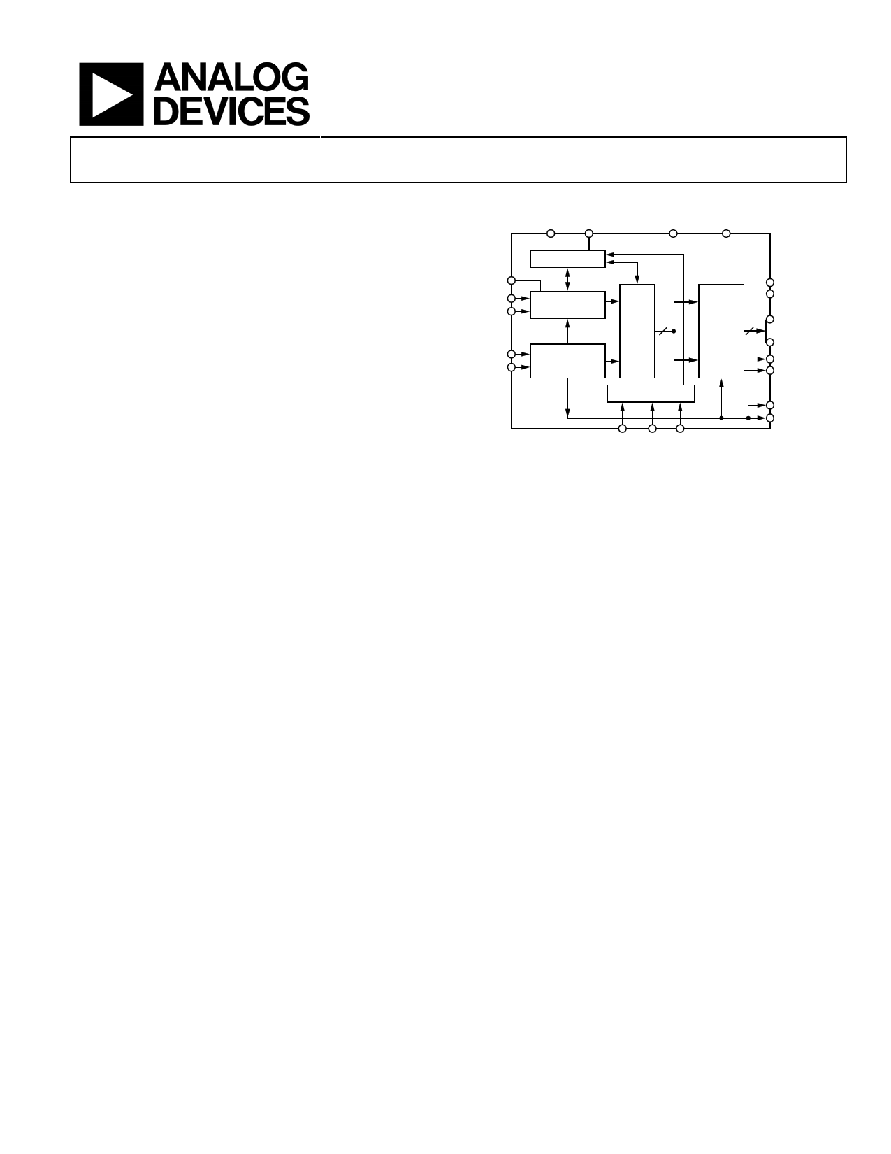
FUNCTIONAL BLOCK DIAGRAM
VREF PWDN
AGND
AVDD
CML
VIN+
VIN–
CLK+
CLK–
REFERENCE
AD9434
TRACK-AND-HOLD
CLOCK
MANAGEMENT
ADC 12
CORE
SERIAL PORT
OUTPUT 12
STAGING
LVDS
SCLK/DFS SDIO CSB
Figure 1.
DRVDD
DRGND
D11± TO D0±
OR+
OR–
DCO+
DCO–
Fabricated on an advanced BiCMOS process, the AD9434 is
available in a 56-lead LFCSP, specified over the industrial
temperature range (−40°C to +85°C). This part is protected
under a U.S. patent.
PRODUCT HIGHLIGHTS
1. High Performance.
Maintains 65 dBFS SNR at 500 MSPS with a 250 MHz input.
2. Low Power.
Consumes only 660 mW at 500 MSPS.
3. Ease of Use.
LVDS output data and output clock signal allow interface
to FPGA technology. The on-chip reference and sample-
and-hold provide flexibility in system design. Use of a
single 1.8 V supply simplifies system power supply design.
4. Serial Port Control.
Standard serial port interface supports various product
functions, such as data formatting, power-down, gain
adjust, and output test pattern generation.
5. The AD9434 is pin compatible with the AD9230, and can
be substituted in many applications with minimal design
changes.
One Technology Way, P.O. Box 9106, Norwood, MA 02062-9106, U.S.A.
Tel: 781.329.4700 ©2011–2013 Analog Devices, Inc. All rights reserved.
Technical Support
www.analog.com
1 page 
AD9434
Data Sheet
AC SPECIFICATIONS
AVDD = 1.8 V, DRVDD = 1.8 V, TMIN = −40°C, TMAX = +85°C, fIN = −1.0 dBFS, full scale = 1.5 V, unless otherwise noted.
Table 2.
Parameter1, 2
SNR
fIN = 30.3 MHz
fIN = 70.3 MHz
fIN = 100.3 MHz
fIN = 250.3 MHz
fIN = 450.3 MHz
SINAD
fIN = 30.3 MHz
fIN = 70.3 MHz
fIN = 100.3 MHz
fIN = 250.3 MHz
fIN = 450.3 MHz
EFFECTIVE NUMBER OF BITS (ENOB)
fIN = 30.3 MHz
fIN = 70.3 MHz
fIN = 100.3 MHz
fIN = 250.3 MHz
fIN = 450.3 MHz
WORST HARMONIC (SECOND or THIRD)
fIN = 30.3 MHz
fIN = 70.3 MHz
fIN = 100.3 MHz
fIN = 250.3 MHz
fIN = 450.3 MHz
SFDR
fIN = 30.3 MHz
fIN = 70.3 MHz
fIN = 100.3 MHz
fIN = 250.3 MHz
fIN = 450.3 MHz
WORST OTHER HARMONIC (SFDR EXCLUDING SECOND and THIRD)
fIN = 30.3 MHz
fIN = 70.3 MHz
fIN = 100.3 MHz
fIN = 250.3 MHz
fIN = 450.3 MHz
TWO-TONE IMD
fIN1 = 119.5 MHz, fIN2 = 122.5 MHz
ANALOG INPUT BANDWIDTH
Full Power
Temp
25°C
25°C
25°C
Full
25°C
25°C
25°C
25°C
25°C
Full
25°C
25°C
25°C
25°C
25°C
25°C
25°C
25°C
25°C
25°C
Full
25°C
25°C
25°C
25°C
25°C
Full
25°C
25°C
25°C
25°C
25°C
Full
25°C
25°C
25°C
25°C
AD9434-370
Min Typ Max
66.3
66.2
66.1
65.3
65.5
64.0
66.1
66.1
66.0
65.2
65.3
63.7
10.7
10.7
10.7
10.6
10.3
−93
−89
−83
−75
−80
−78
89
88
83
75
79
78
−90
−90
−91
−75
−83
−82
−85
1
AD9434-500
Min Typ Max
65.9
65.9
65.8
64.5
65.2
63.5
65.9
65.8
65.8
64.4
64.8
62.9
10.7
10.6
10.6
10.5
10.2
−93
−91
−87
−74
−78
−69
84
82
83
74
78
68
−85
−82
−84
−74
−85
−78
−85
1
Unit
dBFS
dBFS
dBFS
dBFS
dBFS
dBFS
dBFS
dBFS
dBFS
dBFS
dBFS
dBFS
Bits
Bits
Bits
Bits
Bits
dBc
dBc
dBc
dBc
dBc
dBc
dBc
dBc
dBc
dBc
dBc
dBc
dBc
dBc
dBc
dBc
dBc
dBc
dBc
GHz
1 All ac specifications tested by driving CLK+ and CLK− differentially.
2 See the AN-835 Application Note, Understanding High Speed ADC Testing and Evaluation, for a complete set of definitions and how these tests were completed.
Rev. B | Page 4 of 28
5 Page 
AD9434
Pin No.
4
5
6
9
10
11
12
13
14
15
16
17
18
19
20
21
22
Mnemonic
D4+
D5−
D5+
D6−
D6+
D7−
D7+
D8−
D8+
D9−
D9+
D10−
D10+
D11−
D11+
OR−
OR+
Description
D4 True Output.
D5 Complement Output.
D5 True Output.
D6 Complement Output.
D6 True Output.
D7 Complement Output.
D7 True Output.
D8 Complement Output.
D8 True Output.
D9 Complement Output.
D9 True Output.
D10 Complement Output.
D10 True Output.
D11 Complement Output (MSB).
D11 True Output (MSB).
Overrange Complement Output.
Overrange True Output.
1 AGND and DRGND should be tied to a common quiet ground plane.
Data Sheet
Rev. B | Page 10 of 28
11 Page | ||
| Páginas | Total 29 Páginas | |
| PDF Descargar | [ Datasheet AD9434.PDF ] | |
Hoja de datos destacado
| Número de pieza | Descripción | Fabricantes |
| AD9430 | 3.3V A/D Converter | Analog Devices |
| AD9432 | 12-Bit/ 80 MSPS/105 MSPS A/D Converter | Analog Devices |
| AD9433 | IF Sampling ADC | Analog Devices |
| AD9434 | 1.8 V Analog-to-Digital Converter | Analog Devices |
| Número de pieza | Descripción | Fabricantes |
| SLA6805M | High Voltage 3 phase Motor Driver IC. |
Sanken |
| SDC1742 | 12- and 14-Bit Hybrid Synchro / Resolver-to-Digital Converters. |
Analog Devices |
|
DataSheet.es es una pagina web que funciona como un repositorio de manuales o hoja de datos de muchos de los productos más populares, |
| DataSheet.es | 2020 | Privacy Policy | Contacto | Buscar |