|
|
PDF FAN7930C Data sheet ( Hoja de datos )
| Número de pieza | FAN7930C | |
| Descripción | Critical Conduction Mode PFC Controller | |
| Fabricantes | Fairchild Semiconductor | |
| Logotipo | ||
Hay una vista previa y un enlace de descarga de FAN7930C (archivo pdf) en la parte inferior de esta página. Total 22 Páginas | ||
|
No Preview Available !
October 2010
FAN7930C
Critical Conduction Mode PFC Controller
Features
PFC-Ready Signal
Input Voltage Absent Detection
Maximum Switching Frequency Limitation
Internal Soft-Start and Startup without Overshoot
Internal Total Harmonic Distortion (THD) Optimizer
Precise Adjustable Output Over-Voltage Protection
Open-Feedback Protection and Disable Function
Zero-Current Detector (ZCD)
150μs Internal Startup Timer
MOSFET Over-Current Protection (OCP)
Under-Voltage Lockout with 3.5V Hysteresis
Low Startup and Operating Current
Totem-Pole Output with High State Clamp
+500/-800mA Peak Gate Drive Current
8-Pin SOP
Applications
Adapter
Ballast
LCD TV, CRT TV
SMPS
Description
The FAN7930C is an active power factor correction
(PFC) controller for boost PFC applications that operate
in critical conduction mode (CRM). It uses a voltage-
mode PWM that compares an internal ramp signal with
the error amplifier output to generate a MOSFET turn-off
signal. Because the voltage-mode CRM PFC controller
does not need rectified AC line voltage information, it
saves the power loss of an input voltage sensing network
necessary for a current-mode CRM PFC controller.
FAN7930C provides over-voltage protection (OVP),
open-feedback protection, over-current protection
(OCP), input-voltage-absent detection, and under-
voltage lockout protection (UVLO). The PFC-ready pin
can be used to trigger other power stages when PFC
output voltage reaches the proper level with hysteresis.
The FAN7930C can be disabled if the INV pin voltage is
lower than 0.45V and the operating current decreases to
a very low level. Using a new variable on-time control
method, THD is lower than the conventional CRM boost
PFC ICs.
Related Resources
AN-8035 — Design Consideration for Boundary
Conduction Mode PFC Using FAN7930
Ordering Information
www.DataSPheaertt4NUu.cmomber
FAN7930CM
FAN7930CMX
Operating
Temperature Range
-40 to +125°C
Top Mark
Package
FAN7930C 8-Lead Small Outline Package (SOP)
Packing
Method
Rail
Tape & Reel
© 2010 Fairchild Semiconductor Corporation
FAN7930C • Rev. 1.0.0
www.fairchildsemi.com
1 page 
Electrical Characteristics
VCC = 14V, TA = -40°C~+125°C, unless otherwise specified.
Symbol
Parameter
Conditions
VCC Section
VSTART Start Threshold Voltage
VSTOP Stop Threshold Voltage
HYUVLO UVLO Hysteresis
VZ Zener Voltage
VOP Recommended Operating Range
Supply Current Section
VCC Increasing
VCC Decreasing
ICC=20mA
ISTART
Startup Supply Current
IOP Operating Supply Current
IDOP Dynamic Operating Supply Current
IOPDIS
Operating Current at Disable
Error Amplifier Section
VCC=VSTART-0.2V
Output Not Switching
50kHZ, CI=1nF
VINV=0V
VREF1
ΔVREF1
ΔVREF2
IEA,BS
Voltage Feedback Input Threshold1 TA=25°C
Line Regulation
Temperature Stability of VREF1(4)
VCC=14V~20V
Input Bias Current
VINV=1V~4V
IEAS,SR Output Source Current
VINV=VREF -0.1V
IEAS,SK Output Sink Current
VINV=VREF +0.1V
VEAH
Output Upper Clamp Voltage
VINV=1V, VCS=0V
VEAZ
gm
Zero-Duty Cycle Output Voltage
Transconductance(4)
Maximum On-Time Section
tON,MAX1 Maximum On-Time Programming 1 TA=25°C, VZCD=1V
tON,MAX2
Maximum On-Time Programming 2
TA=25°C,
IZCD=0.469mA
Current-Sense Section
VCS
Current-Sense Input Threshold
Voltage Limit
ICS,BS
tCS,D
Input Bias Current
Current-Sense Delay to Output(4)
VCS=0V~1V
dV/dt=1V/100ns,
from 0V to 5V
Min.
11
7.5
3.0
20
13
90
2.465
-0.5
6.0
0.9
90
35.5
11.2
0.7
-1.0
Typ. Max. Units
12 13 V
8.5 9.5 V
3.5 4.0 V
22 24 V
20 V
120 190 µA
1.5 3.0 mA
2.5 4.0 mA
160 230 µA
2.500
0.1
20
-12
12
6.5
1.0
115
2.535
10.0
0.5
7.0
1.1
140
V
mV
mV
µA
µA
µA
V
V
µmho
41.5 47.5 µs
13.0 14.8 µs
0.8 0.9 V
-0.1 1.0 µA
350 500 ns
Continued on the following page…
www.DataSheet4U.com
© 2010 Fairchild Semiconductor Corporation
FAN7930C • Rev. 1.0.0
5
www.fairchildsemi.com
5 Page 
Applications Information
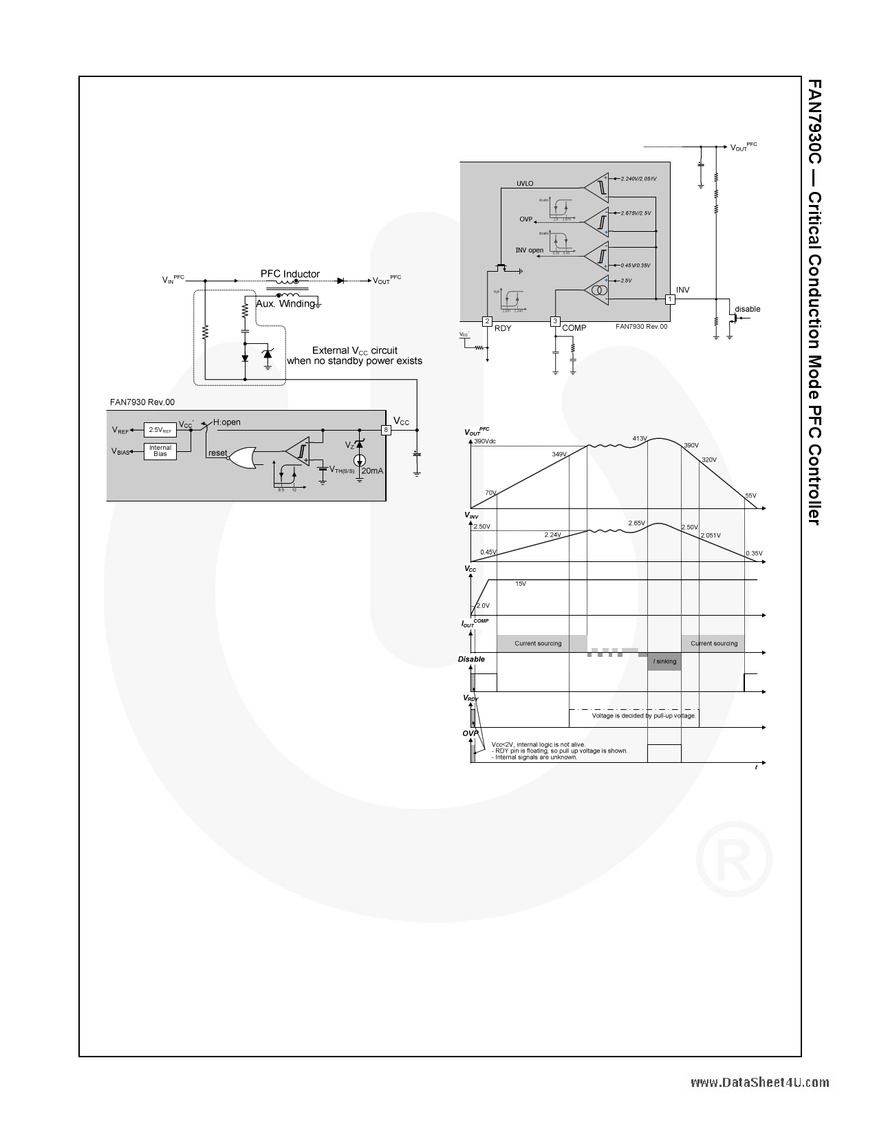
1. Startup: Normally, supply voltage (VCC) of a PFC
block is fed from the additional power supply, which can
be called standby power. Without this standby power,
auxiliary winding for zero current detection can be used
as a supply source. Once the supply voltage of the PFC
block exceeds 12V, internal operation is enabled until
the voltage drops to 8.5V. If VCC exceeds VZ, 20mA
current is sinking from VCC.
Figure 23. Circuit Around INV Pin
Figure 22. Startup Circuit
2. INV Block: Scaled-down voltage from the output is
the input for the INV pin. Many functions are embedded
based on the INV pin: transconductance amplifier,
output OVP comparator, disable comparator, and output
UVLO comparator.
For the output voltage control, a transconductance
amplifier is used instead of the conventional voltage
amplifier. The transconductance amplifier (voltage-
controlled current source) aids the implementation of the
OVP and disable functions. The output current of the
amplifier changes according to the voltage difference of
the inverting and non-inverting input of the amplifier. To
cancel down the line input voltage effect on power factor
correction, the effective control response of the PFC
block should be slower than the line frequency and this
conflicts with the transient response of controller. Two-
pole one-zero type compensation may be used to meet
both requirements.
The OVP comparator shuts down the output drive block
when the voltage of the INV pin is higher than 2.675V
and there is 0.175V hysteresis. The disable comparator
disables operation when the voltage of the inverting
input is lower than 0.35V and there is 100mV hysteresis.
An external small-signal MOSFET can be used to
disable the IC, as shown in Figure 23. The IC operating
www.DatacSuhrereetn4tUd.ceocmreases to reduce power consumption if the
IC is disabled. Error! Reference source not found. is
the timing chart of the internal circuit near the INV pin
when rated PFC output voltage is 390VDC and VCC
supply voltage is 15V.
Figure 24. Timing Chart for INV Block
3. RDY Output: When the INV voltage is higher than
2.24V, RDY output is triggered HIGH and lasts until the
INV voltage is lower than 2.051V. When input AC
voltage is quite high, for example 240VAC, PFC output
voltage is always higher than RDY threshold, regardless
of boost converter operation. In this case, the INV
voltage is already higher than 2.24V before PFC VCC
touches VSTART; however, RDY output is not triggered to
HIGH until VCC touches VSTART. After boost converter
operation stops, RDY is not pulled LOW because the
INV voltage is higher than the RDY threshold. When VCC
of the PFC drops below 5V, RDY is pulled LOW even
though PFC output voltage is higher than threshold. The
RDY pin output is open drain, so needs an external pull-
up resistor to supply the proper power source. The RDY
pin output remains floating until VCC is higher than 2V.
© 2010 Fairchild Semiconductor Corporation
FAN7930C • Rev. 1.0.0
11
www.fairchildsemi.com
11 Page | ||
| Páginas | Total 22 Páginas | |
| PDF Descargar | [ Datasheet FAN7930C.PDF ] | |
Hoja de datos destacado
| Número de pieza | Descripción | Fabricantes |
| FAN7930 | Critical Conduction Mode PFC Controller | Fairchild Semiconductor |
| FAN7930B | Critical Conduction Mode PFC Controller | Fairchild Semiconductor |
| FAN7930C | Critical Conduction Mode PFC Controller | Fairchild Semiconductor |
| Número de pieza | Descripción | Fabricantes |
| SLA6805M | High Voltage 3 phase Motor Driver IC. |
Sanken |
| SDC1742 | 12- and 14-Bit Hybrid Synchro / Resolver-to-Digital Converters. |
Analog Devices |
|
DataSheet.es es una pagina web que funciona como un repositorio de manuales o hoja de datos de muchos de los productos más populares, |
| DataSheet.es | 2020 | Privacy Policy | Contacto | Buscar |
