|
|
|
PDF AD9286 Data sheet ( Hoja de datos )
| Número de pieza | AD9286 | |
| Descripción | 1.8 V Dual Analog-to-Digital Converter (ADC) | |
| Fabricantes | Analog Devices | |
| Logotipo | ||
Hay una vista previa y un enlace de descarga de AD9286 (archivo pdf) en la parte inferior de esta página. Total 28 Páginas | ||
|
No Preview Available !
Data Sheet
FEATURES
Single 1.8 V supply operation
SNR: 49.3 dBFS at 200 MHz input at 500 MSPS
SFDR: 65 dBc at 200 MHz input at 500 MSPS
Low power: 315 mW at 500 MSPS
On-chip interleaved clocking
On-chip reference and track-and-hold
1.2 V p-p analog input range for each channel
Differential input with 500 MHz bandwidth
LVDS-compliant digital output
On-chip voltage reference and sample-and-hold circuit
DNL: ±0.2 LSB
Serial port control options
Interleaved clock timing adjustment
Offset binary, Gray code, or twos complement data format
Optional clock duty cycle stabilizer
Built-in selectable digital test pattern generation
Pin-programmable power-down function
Available in 48-lead LFCSP
APPLICATIONS
Battery-powered instruments
Handheld scope meters
Low cost digital oscilloscopes
OTS: video over fiber
8-Bit, 500 MSPS, 1.8 V
Analog-to-Digital Converter (ADC)
AD9286
GENERAL DESCRIPTION
The AD9286 is an 8-bit, monolithic sampling, analog-to-digital
converter (ADC) that supports interleaved operation and is
optimized for low cost, low power, and ease of use. Each ADC
operates at up to a 250 MSPS conversion rate with outstanding
dynamic performance.
The AD9286 takes a single sample clock and, with an on-chip
clock divider, time interleaves the two ADC cores (each running
at one-half the clock frequency) to achieve the rated 500 MSPS.
By using the SPI, the user can accurately adjust the timing of the
sampling edge per ADC to minimize the image spur energy.
The ADC requires a single 1.8 V supply and an encode clock for
full performance operation. No external reference components
are required for many applications. The digital outputs are LVDS
compatible.
The AD9286 is available in a Pb-free, 48-lead LFCSP that is
specified over the industrial temperature range of −40°C to +85°C.
PRODUCT HIGHLIGHTS
1. Integrated 8-Bit, 500 MSPS ADC.
2. Single 1.8 V Supply Operation with LVDS Outputs.
3. Power-Down Option Controlled via a Pin-Programmable
Setting.
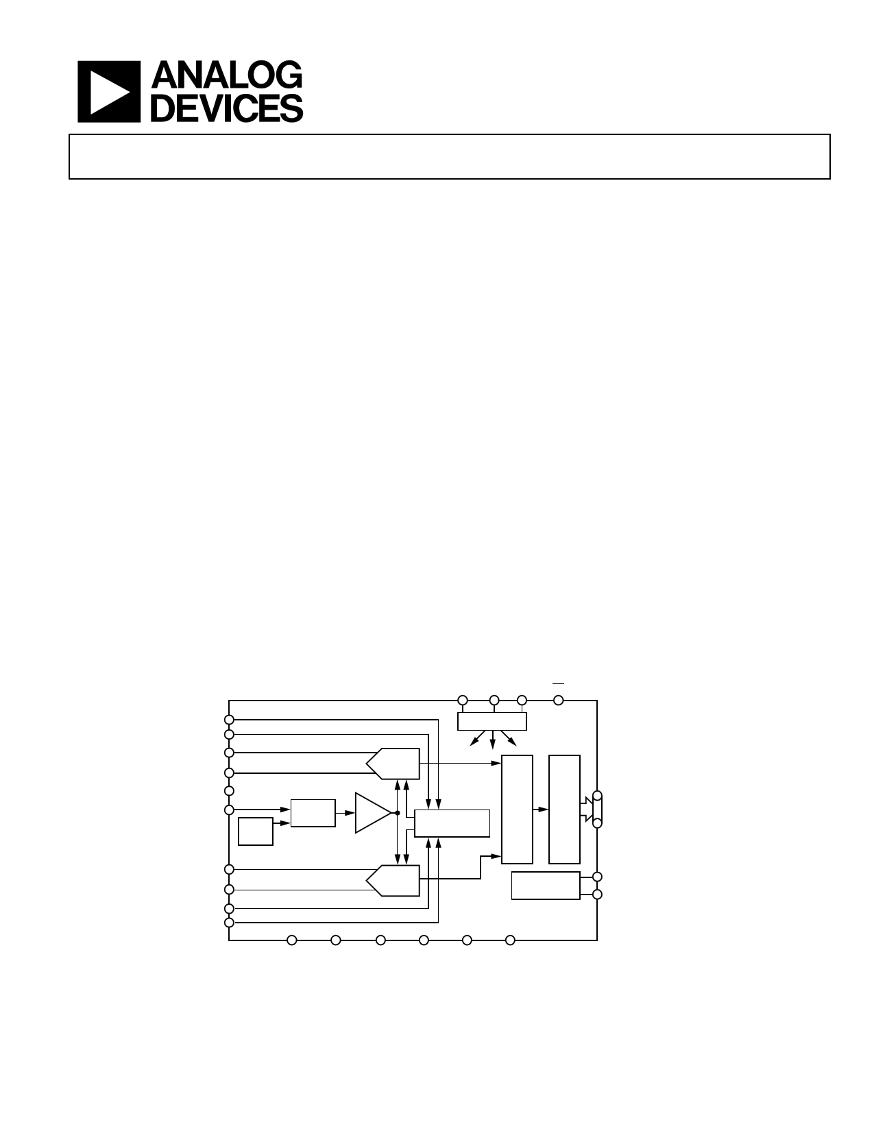
FUNCTIONAL BLOCK DIAGRAM
SDIO/
PWDN CSB SCLK OE
CLK+
CLK–
VIN1+
VIN1–
VCM
VREF
1.0V
VREF
REF
SELECT
ADC
SPI
×1.5 CLOCK
MANAGEMENT
VIN2–
VIN2+
AUXCLK–
AUXCLK+
ADC
DCO
GENERATION
AD9286
RBIAS AUXCLKEN AGND
AVDD DRVDD DRGND
Figure 1.
D7+ (MSB), D7– (MSB)
D0+ (LSB), D0– (LSB)
DCO+
DCO–
Rev. C
Document Feedback
Information furnished by Analog Devices is believed to be accurate and reliable. However, no
responsibility is assumed by Analog Devices for its use, nor for any infringements of patents or other
rights of third parties that may result from its use. Specifications subject to change without notice. No
license is granted by implication or otherwise under any patent or patent rights of Analog Devices.
Trademarksandregisteredtrademarksarethepropertyoftheirrespectiveowners.
One Technology Way, P.O. Box 9106, Norwood, MA 02062-9106, U.S.A.
Tel: 781.329.4700 ©2011–2015 Analog Devices, Inc. All rights reserved.
Technical Support
www.analog.com
1 page 
AD9286
Data Sheet
AC SPECIFICATIONS
AVDD = 1.8 V, DRVDD = 1.8 V, 1.0 V internal ADC reference, VIN = −1.0 dBFS differential input, optimum timing value set, unless
otherwise noted.
Table 2.
Parameter
Temperature
Min
Typ
Max Unit
SIGNAL-TO-NOISE RATIO (SNR)
fIN = 10.3 MHz
25°C
49.3
dBFS
fIN = 70 MHz
25°C 49.3 dBFS
fIN = 96.6 MHz
Full 48.8 49.3
dBFS
fIN = 220 MHz
25°C
49.3
dBFS
SIGNAL-TO-NOISE-AND-DISTORTION (SINAD)
fIN = 10.3 MHz
25°C
49.2
dBFS
fIN = 70 MHz
25°C 49.2 dBFS
fIN = 96.6 MHz
Full 48.7 49.2
dBFS
fIN = 220 MHz
25°C
49.2
dBFS
EFFECTIVE NUMBER OF BITS (ENOB)
fIN = 10.3 MHz
25°C
7.9
Bits
fIN = 70 MHz
25°C 7.9
Bits
fIN = 96.6 MHz
Full 7.8 7.9
Bits
fIN = 220 MHz
25°C
7.9
Bits
WORST SECOND OR THIRD HARMONIC
fIN = 10.3 MHz
25°C
−70
dBc
fIN = 70 MHz
25°C −70
dBc
fIN = 96.6 MHz
Full
−69 −61 dBc
fIN = 220 MHz
25°C
−65
dBc
SPURIOUS-FREE DYNAMIC RANGE (SFDR)1
fIN = 10.3 MHz
25°C
70
dBc
fIN = 70 MHz
25°C 70
dBc
fIN = 96.6 MHz
Full 61 68
dBc
fIN = 220 MHz
25°C
65
dBc
WORST OTHER HARMONIC OR SPUR
fIN = 10.3 MHz
25°C
−71
dBc
fIN = 70 MHz
25°C −71
dBc
fIN = 96.6 MHz
Full
−71 −64 dBc
fIN = 220 MHz
25°C
−67
dBc
CROSSTALK
Full −80 dBc
1 Excludes offset and alias spur (see the Interleave Performance section).
Rev. C | Page 4 of 27
5 Page 
AD9286
PIN CONFIGURATION AND FUNCTION DESCRIPTIONS
Data Sheet
AVDD 1
AVDD 2
AUXCLK+ 3
AUXCLK– 4
RBIAS 5
AUXCLKEN 6
DRGND 7
DRVDD 8
D0– (LSB) 9
D0+ (LSB) 10
D1– 11
D1+ 12
PIN 1
INDICATOR
AD9286
TOP VIEW
(Not to Scale)
36 AVDD
35 AVDD
34 CLK+
33 CLK–
32 CSB
31 SDIO/PWDN
30 SCLK
29 OE
28 DRGND
27 DRVDD
26 D7+ (MSB)
25 D7– (MSB)
NOTES
1. THE EXPOSED PADDLE MUST BE SOLDERED TO THE PCB ANALOG
GROUND TO ENSURE PROPER FUNCTIONALITY AND HEAT
DISSIPATION, NOISE, AND MECHANICAL STRENGTH BENEFITS.
Figure 6. Pin Configuration
Table 8. Pin Function Descriptions
Pin No.
Mnemonic
ADC Power Pins
1, 2, 35, 36, 37, 40, 42,
44, 45, 48
AVDD
8, 27 DRVDD
7, 28 DRGND
0 AGND
ADC Analog Pins
39
38
46
47
43
5
41
34
33
3
4
Digital Inputs
6
29
Digital Outputs
26
25
24
23
22
21
VIN1+
VIN1−
VIN2+
VIN2−
VREF
RBIAS
VCM
CLK+
CLK−
AUXCLK+
AUXCLK−
AUXCLKEN
OE
D7+ (MSB)
D7− (MSB)
D6+
D6−
D5+
D5−
Type
Description
Supply
Supply
Ground
Ground
Analog Power Supply (1.8 V Nominal).
Digital Output Driver Supply (1.8 V Nominal).
Digital Output Ground.
Analog Ground. Pin 0 is the exposed thermal pad on the bottom of the
package. This is the only ground connection, and it must be soldered to
the PCB analog ground to ensure proper functionality and heat dissipation,
noise, and mechanical strength benefits.
Input
Input
Input
Input
Input/output
Input/output
Output
Input
Input
Input
Input
Differential Analog Input Pin (+) for Channel 1.
Differential Analog Input Pin (−) for Channel 1.
Differential Analog Input Pin (+) for Channel 2.
Differential Analog Input Pin (−) for Channel 2.
Voltage Reference Input/Output.
External Reference Bias Resistor. Connect 10 kΩ from RBIAS to AGND.
Common-Mode Level Bias Output for Analog Inputs.
ADC Clock Input—True.
ADC Clock Input—Complement.
Auxiliary ADC Clock Input—True.
Auxiliary ADC Clock Input—Complement.
Input
Input
Auxiliary Clock Input Enable.
Digital Enable (Active Low) to Tristate Output Data Pins.
Output
Output
Output
Output
Output
Output
Output Data 7—True.
Output Data 7—Complement.
Output Data 6—True.
Output Data 6—Complement.
Output Data 5—True.
Output Data 5—Complement.
Rev. C | Page 10 of 27
11 Page | ||
| Páginas | Total 28 Páginas | |
| PDF Descargar | [ Datasheet AD9286.PDF ] | |
Hoja de datos destacado
| Número de pieza | Descripción | Fabricantes |
| AD9280 | CMOS A/D Converter | Analog Devices |
| AD9281 | Dual Channel 8-Bit Resolution CMOS ADC | Analog Devices |
| AD9283 | 3V A/D Converter | Analog Devices |
| AD9284 | 1.8 V Dual Analog-to-Digital Converter (ADC) | Analog Devices |
| Número de pieza | Descripción | Fabricantes |
| SLA6805M | High Voltage 3 phase Motor Driver IC. |
Sanken |
| SDC1742 | 12- and 14-Bit Hybrid Synchro / Resolver-to-Digital Converters. |
Analog Devices |
|
DataSheet.es es una pagina web que funciona como un repositorio de manuales o hoja de datos de muchos de los productos más populares, |
| DataSheet.es | 2020 | Privacy Policy | Contacto | Buscar |