|
|
|
PDF PCS3P624Z09C Data sheet ( Hoja de datos )
| Número de pieza | PCS3P624Z09C | |
| Descripción | Low Frequency Timing-Safe Peak EMI reduction IC | |
| Fabricantes | PulseCore Semiconductor | |
| Logotipo | ||
Hay una vista previa y un enlace de descarga de PCS3P624Z09C (archivo pdf) en la parte inferior de esta página. Total 15 Páginas | ||
|
No Preview Available !
May 2008
rev 0.1
PCS3P624Z05B/C
PCS3P624Z09B/C
High Frequency Timing-Safe™ Peak EMI reduction IC
General Features
• High Frequency Clock distribution with Timing-
Safe™ Peak EMI Reduction
• Input frequency range: 50MHz - 100MHz
• Multiple low skew Timing-safe™ Outputs:
PCS3P624Z05: 5 Outputs
PCS3P624Z09: 9 Outputs
• External Input-Output Delay Control option
• Supply Voltage: 3.3V±0.3V
• Commercial and Industrial temperature range
• Packaging Information:
ASM3P624Z05: 8 pin SOIC, and TSSOP
ASM3P624Z09:16 pin SOIC, and TSSOP
• True Drop-in Solution for Zero Delay Buffer,
ASM5P2305A / 09A
Functional Description
PCS3P624Z05/09 is a versatile, 3.3V Zero-delay buffer
designed to distribute high frequency Timing-Safe™ clocks
www.DataSheet4U.com
with Peak EMI reduction. PCS3P624Z05 is an eight-pin
version, accepts one reference input and drives out five
low-skew Timing-Safe™ clocks. PCS3P624Z09 accepts
one reference input and drives out nine low-skew Timing-
Safe™clocks.
PCS3P624Z05/09 has a DLY_CTRL for adjusting the
Input-Output clock delay, depending upon the value of
capacitor connected at this pin to GND.
PCS3P624Z05/09 operates from a 3.3V supply and is
available in two different packages, as shown in the
ordering information table, over commercial and Industrial
temperature range.
Application
PCS3P624Z05/09 is targeted for use in Displays and
memory interface systems.
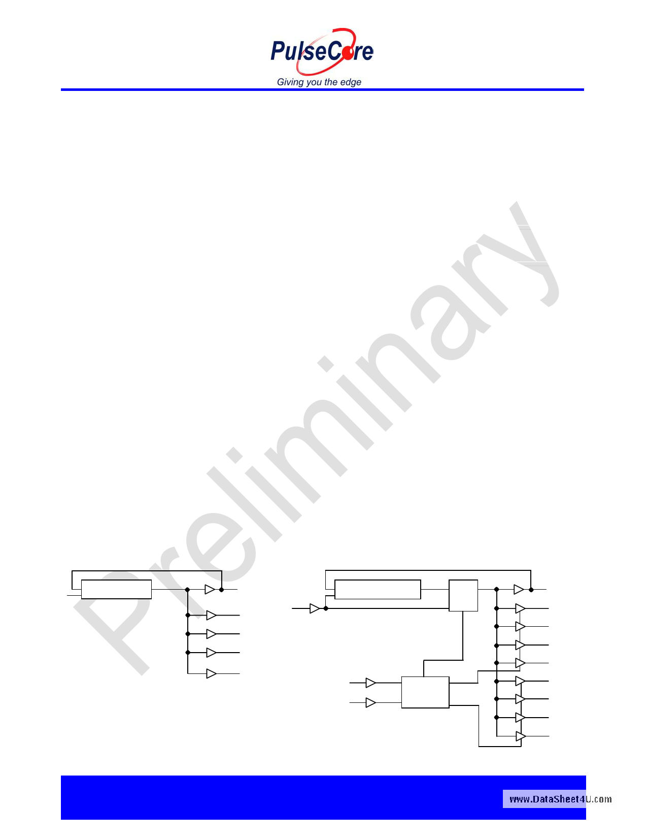
General Block Diagram
CLKIN
PLL
PCS3P624Z05B/C
DLY_CTRL
PLL MUX
CLKOUT1 CLKIN
CLKOUT2
CLKOUT3
CLKOUT4
S2
S1
Select Input
Decoding
PCS3P624Z09B/C
DLY_CTRL
CLKOUTA1
CLKOUTA2
CLKOUTA3
CLKOUTA4
CLKOUTB1
CLKOUTB2
CLKOUTB3
CLKOUTB4
PulseCore Semiconductor Corporation
1715 S. Bascom Ave Suite 200 Campbell, CA 95008 • Tel: 408-879-9077 • Fax: 408-879-9018
www.pulsecoresemi.com
Notice: The information in this document is subject to change without notice.
1 page 
May 2008
rev 0.1
PCS3P624Z05B/C
PCS3P624Z09B/C
Select Input Decoding table for PCS3P624Z09
www.DataSheet4U.com
S2
S1 CLKOUT A1 - A4 CLKOUT B1 - B4 DLY_CTRL1 Output Source
PLL
Shut-Down
0
0
Three-state
Three-state
Driven
PLL
N
01
Driven
Three-state
Driven
PLL
N
10
Driven
Driven
Driven
Reference
Y
11
Driven
Driven
Driven
PLL
N
Notes: This output is driven and has an internal feedback for the PLL. The load on this output can be adjusted to change the skew between the reference and
the Output.
Spread Spectrum Control and Input-Output Skew Table
Frequency (MHz)
Device
PCS3P624Z05B / 09B
75
PCS3P624Z05C / 09C
Note: TSKEW is measured in units of the Clock Period
Absolute Maximum Ratings
Deviation (±%)
0.25
0.5
Input-Output Skew (±TSKEW)
0.0625
0.125
Symbol
VDD
VIN
TSTG
Ts
TJ
TDV
Parameter
Supply Voltage to Ground Potential
DC Input Voltage (CLKIN)
Storage temperature
Max. Soldering Temperature (10 sec)
Junction Temperature
Static Discharge Voltage (As per JEDEC STD22- A114-B)
Rating
-0.5 to +4.6
-0.5 to +7
-65 to +125
260
150
2
Unit
V
°C
°C
°C
KV
Note: These are stress ratings only and are not implied for functional use. Exposure to absolute maximum ratings for prolonged periods of time may affect
device reliability.
Operating Conditions
Parameter
Description
VDD
Supply Voltage
TA Operating Temperature (Ambient Temperature)
CL Load Capacitance
CIN Input Capacitance
Min Max Unit
3.0 3.6 V
-40 +85 °C
30 pF
7 pF
High Frequency Timing-Safe™ Peak EMI Reduction IC
Notice: The information in this document is subject to change without notice.
5 of 15
5 Page 
May 2008
rev 0.1
8
PCS3P624Z05B/C
PCS3P624Z09B/C
16-lead (150 Mil) Molded SOIC Package
1 PIN 1 ID
EH
www.DataSheet4U.com
9 16
D
e
B
Seating Plane
A2
A
0.004
A1
θ
h
C
L
Symbol
A
A1
A2
B
C
D
E
e
H
h
L
θ
Dimensions
Inches
Millimeters
Min Max Min Max
0.053
0.069
1.35
1.75
0.004
0.010
0.10
0.25
0.049
0.059
1.25
1.50
0.013
0.022
0.33
0.53
0.008
0.012
0.19
0.27
0.386
0.394
9.80
10.01
0.150
0.157
3.80
4.00
0.050 BSC
1.27 BSC
0.228
0.244
5.80
6.20
0.010
0.016
0.25
0.41
0.016
0.035
0.40
0.89
0° 8° 0° 8°
High Frequency Timing-Safe™ Peak EMI Reduction IC
Notice: The information in this document is subject to change without notice.
11 of 15
11 Page | ||
| Páginas | Total 15 Páginas | |
| PDF Descargar | [ Datasheet PCS3P624Z09C.PDF ] | |
Hoja de datos destacado
| Número de pieza | Descripción | Fabricantes |
| PCS3P624Z09B | Low Frequency Timing-Safe Peak EMI reduction IC | PulseCore Semiconductor |
| PCS3P624Z09C | Low Frequency Timing-Safe Peak EMI reduction IC | PulseCore Semiconductor |
| Número de pieza | Descripción | Fabricantes |
| SLA6805M | High Voltage 3 phase Motor Driver IC. |
Sanken |
| SDC1742 | 12- and 14-Bit Hybrid Synchro / Resolver-to-Digital Converters. |
Analog Devices |
|
DataSheet.es es una pagina web que funciona como un repositorio de manuales o hoja de datos de muchos de los productos más populares, |
| DataSheet.es | 2020 | Privacy Policy | Contacto | Buscar |