|
|
|
PDF AD9467 Data sheet ( Hoja de datos )
| Número de pieza | AD9467 | |
| Descripción | Analog-to-Digital Converter | |
| Fabricantes | Analog Devices | |
| Logotipo | ||
Hay una vista previa y un enlace de descarga de AD9467 (archivo pdf) en la parte inferior de esta página. Total 30 Páginas | ||
|
No Preview Available !
Data Sheet
FEATURES
75.5 dBFS SNR to 210 MHz at 250 MSPS
90 dBFS SFDR to 300 MHz at 250 MSPS
SFDR at 170 MHz at 250 MSPS
92 dBFS at −1 dBFS
100 dBFS at −2 dBFS
60 fs rms jitter
Excellent linearity at 250 MSPS
DNL = ±0.5 LSB typical
INL = ±3.5 LSB typical
2 V p-p to 2.5 V p-p (default) differential full-scale
input (programmable)
Integrated input buffer
External reference support option
Clock duty cycle stabilizer
Output clock available
Serial port control
Built-in selectable digital test pattern generation
Selectable output data format
LVDS outputs (ANSI-644 compatible)
1.8 V and 3.3 V supply operation
APPLICATIONS
Multicarrier, multimode cellular receivers
Antenna array positioning
Power amplifier linearization
Broadband wireless
Radar
Infrared imaging
Communications instrumentation
GENERAL DESCRIPTION
The AD9467 is a 16-bit, monolithic, IF sampling analog-to-
digital converter (ADC). It is optimized for high performance
over wide bandwidths and ease of use. The product operates at a
250 MSPS conversion rate and is designed for wireless receivers,
instrumentation, and test equipment that require a high
dynamic range.
The ADC requires 1.8 V and 3.3 V power supplies and a low
voltage differential input clock for full performance operation.
No external reference or driver components are required for
many applications. Data outputs are LVDS compatible (ANSI-644
compatible) and include the means to reduce the overall current
needed for short trace distances.
Rev. D
Document Feedback
Information furnished by Analog Devices is believed to be accurate and reliable. However, no
responsibilityisassumedbyAnalogDevices for itsuse,nor foranyinfringementsofpatentsor other
rights of third parties that may result from its use. Specifications subject to change without notice. No
license is granted by implication or otherwise under any patent or patent rights of Analog Devices.
Trademarksandregisteredtrademarksarethepropertyoftheirrespectiveowners.
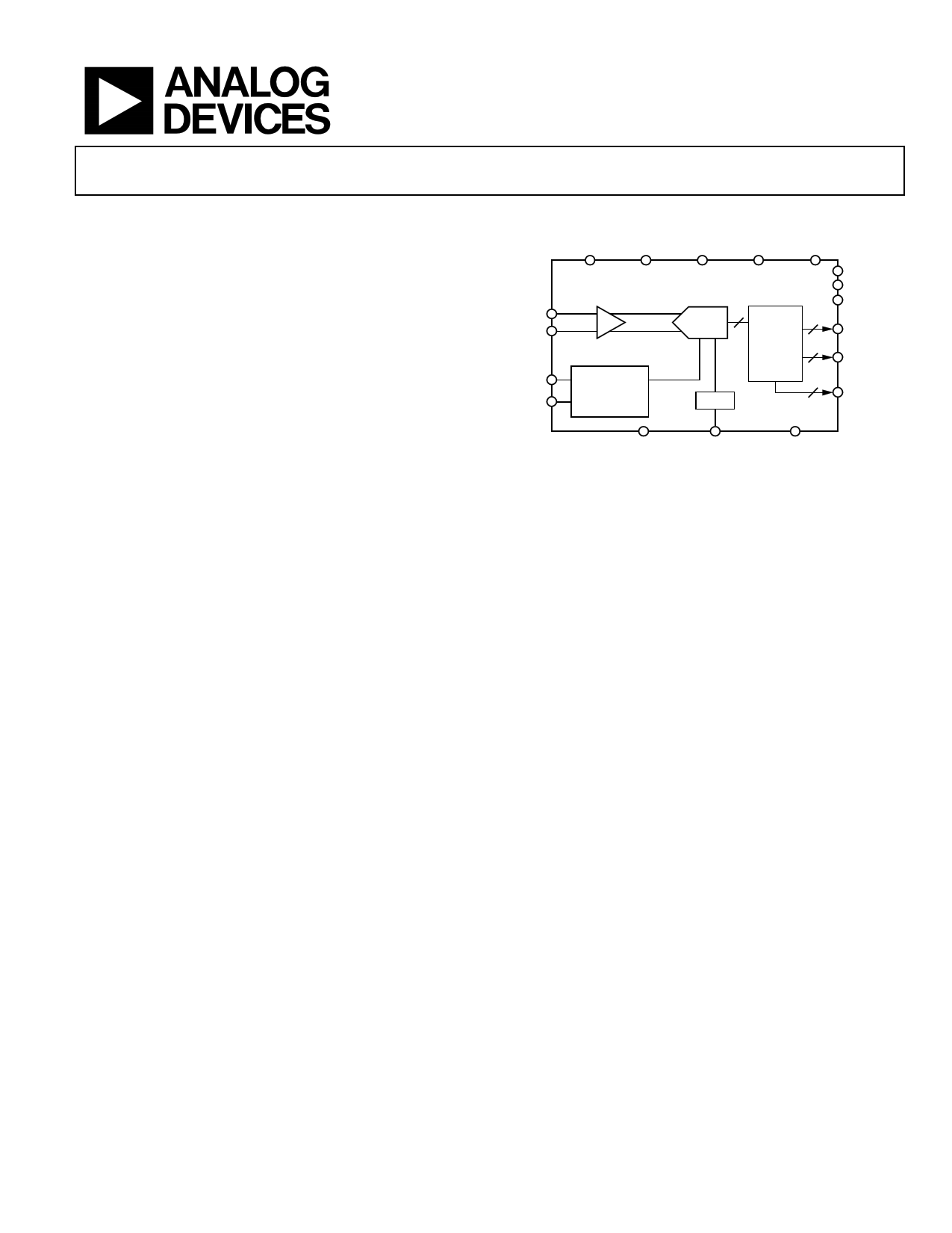
16-Bit, 200 MSPS/250 MSPS
Analog-to-Digital Converter
AD9467
VIN+
VIN–
CLK+
CLK–
FUNCTIONAL BLOCK DIAGRAM
AVDD1
(1.8V)
AVDD2
(3.3V)
AVDD3
SPIVDD DRVDD
(1.8V) (1.8V TO 3.3V) (1.8V)
AD9467
BUFFER
CLOCK
AND TIMING
MANAGEMENT
PIPELINE 16
ADC
LVDS
OUTPUT
STAGING
2
16
2
REF
CSB
SDIO
SCLK
OR+/OR–
D15+/D15–
TO
D0+/D0–
DCO+/DCO–
AGND
XVREF
Figure 1.
DRGND
A data clock output (DCO) for capturing data on the output is
provided for signaling a new output bit.
The internal power-down feature supported via the SPI typically
consumes less than 5 mW when disabled.
Optional features allow users to implement various selectable
operating conditions, including input range, data format select,
and output data test patterns.
The AD9467 is available in a Pb-free, 72-lead, LFCSP specified
over the −40°C to +85°C industrial temperature range.
PRODUCT HIGHLIGHTS
1. IF optimization capability used to improve SFDR.
2. Outstanding SFDR performance for IF sampling
applications such as multicarrier, multimode 3G, and 4G
cellular base station receivers.
3. Ease of use: on-chip reference, high input impedance
buffer, adjustable analog input range, and an output clock
to simplify data capture.
4. Packaged in a Pb-free, 72-lead LFCSP package.
5. Clock duty cycle stabilizer (DCS) maintains overall ADC
performance over a wide range of input clock pulse widths.
6. Standard serial port interface (SPI) supports various
product features and functions, such as data formatting
(offset binary, twos complement, or Gray coding).
One Technology Way, P.O. Box 9106, Norwood, MA 02062-9106, U.S.A.
Tel: 781.329.4700 ©2010–2013 Analog Devices, Inc. All rights reserved.
Technical Support
www.analog.com
1 page 
AD9467
Data Sheet
AC SPECIFICATIONS
AVDD1 = 1.8 V, AVDD2 = 3.3 V, AVDD3 = 1.8 V, DRVDD = 1.8 V, specified maximum sampling rate, 2.5 V p-p differential input,
1.25 V internal reference, AIN = −1.0 dBFS, DCS on, default SPI settings, unless otherwise noted.
Table 2.
Parameter1
ANALOG INPUT FULL SCALE
SIGNAL-TO-NOISE RATIO (SNR)
fIN = 5 MHz
fIN = 97 MHz
fIN = 97 MHz
fIN = 140 MHz
fIN = 170 MHz
fIN = 170 MHz
fIN = 210 MHz
fIN = 300 MHz
SIGNAL-TO-NOISE AND DISTORTION RATIO (SINAD)
fIN = 5 MHz
fIN = 97 MHz
fIN = 97 MHz
fIN = 140 MHz
fIN = 170 MHz
fIN = 170 MHz
fIN = 210 MHz
fIN = 300 MHz
EFFECTIVE NUMBER OF BITS (ENOB)
fIN = 5 MHz
fIN = 97 MHz
fIN = 97 MHz
fIN = 140 MHz
fIN = 170 MHz
fIN = 170 MHz
fIN = 210 MHz
fIN = 300 MHz
SPURIOUS-FREE DYNAMIC RANGE (SFDR) (INCLUDING
SECOND AND THIRD HARMONIC DISTORTION)2
fIN = 5 MHz
fIN = 97 MHz
fIN = 97 MHz
fIN = 140 MHz
fIN = 170 MHz
fIN = 170 MHz
fIN = 210 MHz
fIN = 300 MHz
SPURIOUS-FREE DYNAMIC RANGE (SFDR) (INCLUDING SECOND
AND THIRD HARMONIC DISTORTION)2
fIN = 5 MHz @ −2 dB Full Scale
fIN = 97 MHz @ −2 dB Full Scale
fIN = 140 MHz @ −2 dB Full Scale
fIN = 170 MHz @ −2 dB Full Scale
fIN = 210 MHz @ −2 dB Full Scale
fIN = 300 MHz @ −2 dB Full Scale
Temp
25°C
25°C
Full
25°C
25°C
Full
25°C
25°C
25°C
25°C
Full
25°C
25°C
Full
25°C
25°C
25°C
25°C
Full
25°C
25°C
Full
25°C
25°C
25°C
25°C
Full
25°C
25°C
Full
25°C
25°C
Full
Full
Full
Full
Full
Full
AD9467BCPZ-200
Min Typ
Max
2.5 2/2.5
74.6/76.4
75.1 74.5/76.2
73.8
74.3/76.0
74.2/75.8
73.9/75.5
73.5/74.7
74.6/76.3
74.7 74.5/76.2
73.1
74.3/75.9
74.1/75.6
73.9/75.3
73.3/74.3
12.1/12.4
12.1/12.4
12.1/12.3
12.0/12.3
12.0/12.2
11.9/12.0
95/95
86 95/95
83
94/93
95/90
93/88
92/86
100/96
100/98
98/96
96/93
94/93
90/89
AD9467BCPZ-250
Min Typ
Max
2.5 2/2.5
74.7/76.4
74.5/76.1
74.4/76.0
74.7 74.3/75.8
72.3
74.0/75.5
73.3/74.6
74.6/76.3
74.4/76.0
74.4/76.0
74.4 74.2/75.8
71.8
73.9/75.4
73.1/74.4
12.1/12.4
12.1/12.3
12.1/12.3
12.0/12.3
12.0/12.2
11.9/12.1
98/97
95/93
94/95
84 93/92
84
93/92
93/90
100/100
97/97
100/95
100/100
93/93
90/90
Unit
V p-p
dBFS
dBFS
dBFS
dBFS
dBFS
dBFS
dBFS
dBFS
dBFS
dBFS
dBFS
dBFS
dBFS
dBFS
dBFS
dBFS
Bits
Bits
Bits
Bits
Bits
Bits
Bits
Bits
dBFS
dBFS
dBFS
dBFS
dBFS
dBFS
dBFS
dBFS
dBFS
dBFS
dBFS
dBFS
dBFS
dBFS
Rev. D | Page 4 of 32
5 Page 
AD9467
Pin No.
36
27
28
39
40
47
48
49
50
57
Mnemonic
D15+/D14+
DCO−
DCO+
OR−
OR+
DNC
SDIO
SCLK
CSB
XVREF
Description
D15 (MSB) and D14 Digital Output True.
Data Clock Digital Output Complement.
Data Clock Digital Output True.
Out-of-Range Digital Output Complement.
Out-of-Range Digital Output True.
Do Not Connect (Leave Pin Floating).
Serial Data Input/Output.
Serial Clock.
Chip Select Bar.
External VREF Option.
Data Sheet
Rev. D | Page 10 of 32
11 Page | ||
| Páginas | Total 30 Páginas | |
| PDF Descargar | [ Datasheet AD9467.PDF ] | |
Hoja de datos destacado
| Número de pieza | Descripción | Fabricantes |
| AD9460 | 80 MSPS/105 MSPS ADC | Analog Devices |
| AD9461 | IF Sampling ADC | Analog Devices |
| AD9467 | Analog-to-Digital Converter | Analog Devices |
| Número de pieza | Descripción | Fabricantes |
| SLA6805M | High Voltage 3 phase Motor Driver IC. |
Sanken |
| SDC1742 | 12- and 14-Bit Hybrid Synchro / Resolver-to-Digital Converters. |
Analog Devices |
|
DataSheet.es es una pagina web que funciona como un repositorio de manuales o hoja de datos de muchos de los productos más populares, |
| DataSheet.es | 2020 | Privacy Policy | Contacto | Buscar |