|
|
PDF BD8166EFV Data sheet ( Hoja de datos )
| Número de pieza | BD8166EFV | |
| Descripción | 12V Input Multi-channel System Power Supply IC | |
| Fabricantes | ROHM Semiconductor | |
| Logotipo | ||
Hay una vista previa y un enlace de descarga de BD8166EFV (archivo pdf) en la parte inferior de esta página. Total 18 Páginas | ||
|
No Preview Available !
Power Supply IC Series for TFT-LCD Panels
12V Input Multi-channel
System Power Supply IC
BD8166EFV
No.09035EBT14
●Description
The BD8166EFV is a system power supply for the TFT-LCD panels used for liquid crystal TVs.
Incorporates two high-power FETs with low on resistance for large currents that employ high-power packages, thus driving
large current loads while suppressing the generation of heat. A charge pump controller is incorporated as well, thus greatly
reducing the number of application components.
●Features
1) Step-up and step-down DC/DC converter
2) Incorporates 2-A N-channel FET.
3) Incorporates positive/negative charge pumps.
4) Incorporates a gate shading function.
5) Input voltage limit: 6 V to 18 V
6) Feedback voltage: 1.25 V ± 1.6%
7) Switching frequency: 500 kHz
8) Protection circuit: Undervoltage lockout protection circuit
Thermal shutdown circuit
Overcurrent protection circuit
Short protection circuit of timer latch type
9) HTSSOP-B40 Package
●Applications
Power supply for the TFT-LCD panels used for LCD TVs
●Absolute maximum ratings (Ta = 25℃)
Parameter
Symbol
Limit
Power supply voltage
Vcc, PVCC
19
Vo1 voltage
Vo1 19
Vo2 voltage
Vo2 40
IG Voltage
IGH 7
Maximum junction temperature
Tjmax
150
Power dissipation
Pd 4700*1
Operating temperature range Topr -40 to 85
Storage temperature range
Tstg -55 to 150
* Reduced by 37.6 mW/℃ over 25℃, when mounted on a glass epoxy 4-layer board (70 mm 70 mm 1.6 mm)
(Copper foil on back 70 mm 70 mm).
Unit
V
V
V
V
℃
mW
℃
℃
●Recommended Operating Ranges (Ta = 25℃)
Parameter
Symbol
Power supply voltage
Vo1 voltage
Vo2 voltage
I G Voltage
SW current
VCC, PVCC
Vo1
Vo2
IGH
SW1, SW2
Limit
Min. Max.
6 18
8 18
— 39
—5
—2
Unit
V
V
V
V
A
www.rohm.com
© 2009 ROHM Co., Ltd. All rights reserved.
1/17
2009.07 - Rev.B
1 page 
BD81666EFV
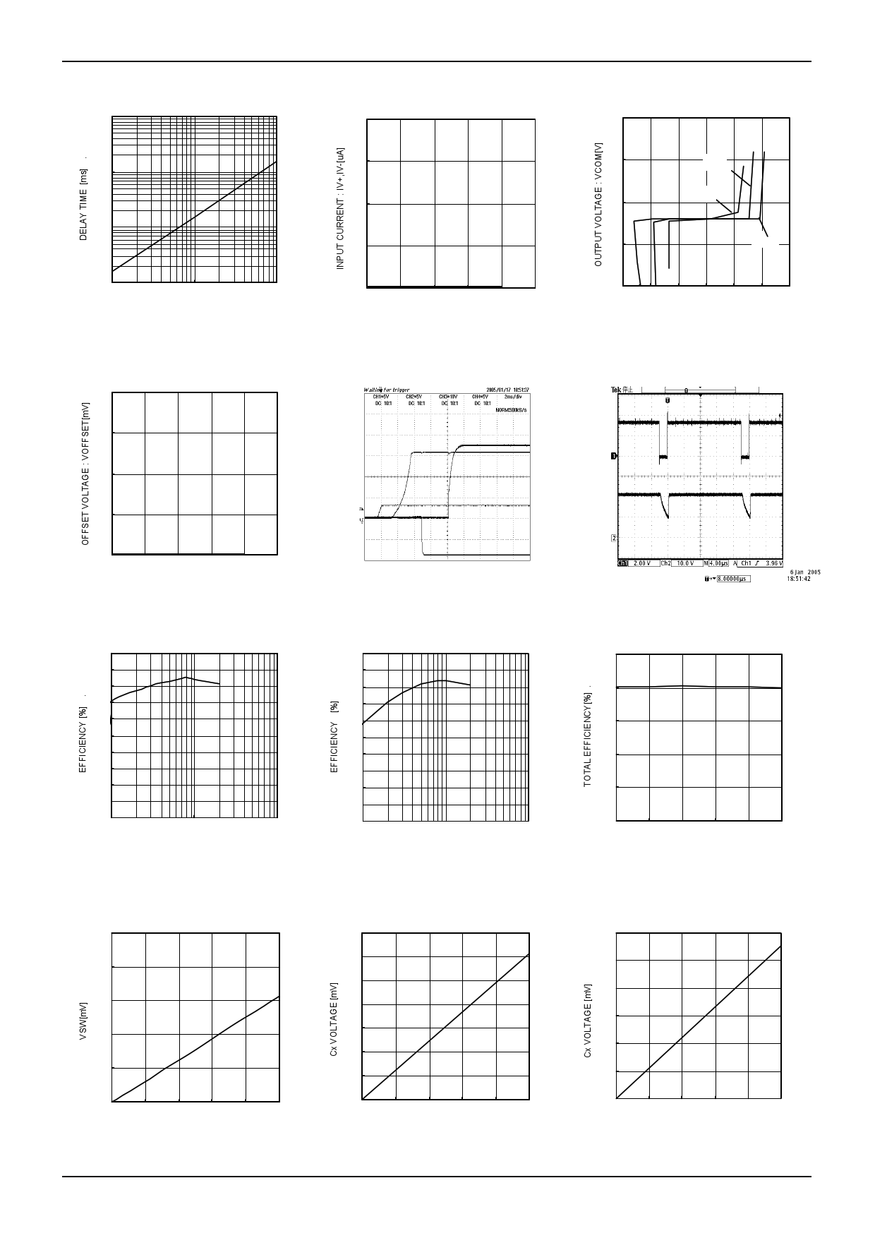
●Reference Data (Unless otherwise specified, Ta = 25℃)
100 1.6
10
1
0.1
0.001
0.01
SCP CAPACITOR [μF]
0.1
Fig.13 SCP Capacity
vs Delay Time
1.6
1.2
0.8
0.4
0
0 5 10 15 20 25
INPUT VOLTAGE : V+,V- [V]
Fig.14 COM Input Bias Current
1.2
0.8
0.4
0
0 5 10 15 20 25
VCOM VOLTAGE : VCOM[V]
Fig.16 VCOM Offset Voltage
15V
3.3V
35V
-6V
Fig.17 Start-up Sequence
100
90
80
70
60
50
40
30
20
10
0
100
1000
OUTPUT CURRENT[mA]
10000
Fig.19 Output Current vs
Efficiency (Vo1)
400
320
240
160
80
0
0 200 400 600 800 1000
ISW[mA]
Fig.22 DC/DC SW On Resistance
www.rohm.com
© 2009 ROHM Co., Ltd. All rights reserved.
100
90
80
70
60
50
40
30
20
10
0
100
1000
OUTPUT CURRENT[mA]
10000
Fig.20 Output Current vs
Efficiency (VDD)
140
120
100
80
60
40
20
0
0 20 40 60 80 100
Cx CURRENT [mA]
Fig.23 Charge Pump N-channel
On Resistance
5/17
Technical Note
20
15 25℃
85℃
10
5 -40℃
0
-300
-200 -100 0 100 200
OUTPUT CURRENT : ICOM[mA]
300
Fig.15 COM Load Regulation
IG
Vo2GS
Fig.18 Gate-shading Waveform
100
80
60
40
20
0
8 10 12 14 16 18
SUPPLY VOLTAGE[V]
Fig.21 Total Efficiency
180
150
120
90
60
30
0
0 20 40 60 80 100
Cx CURRENT [mA]
Fig.24 Charge Pump
P-channel On Resistance
2009.07 - Rev.B
5 Page 
BD81666EFV
Technical Note
(3) Phase compensation
Phase Setting Method
The following conditions are required in order to ensure the stability of the negative feedback circuit.
Phase lag should be 150° or lower during gain 1 (0 dB) (phase margin of 30° or higher).
Because DC/DC converter applications are sampled using the switching frequency, the overall GBW should be set to
1/10 the switching frequency or lower. The target application characteristics can be summarized as follows:
Phase lag should be 150° or lower during gain 1 (0 dB) (phase margin of 30° or higher).
The GBW at that time (i.e., the frequency of a 0-dB gain) is 1/10 of the switching frequency or below.
In other words, because the response is determined by the GBW limitation, it is necessary to use higher switching
frequencies to raise response.
One way to maintain stability through phase compensation involves canceling the secondary phase lag (-180°) caused
by LC resonance with a secondary phase advance (by inserting 2 phase advances).
The GBW (i.e., the frequency with the gain set to 1) is determined by the phase compensation capacitance connected to
the error amp. Increase the capacitance if a GBW reduction is required.
(a) Standard integrator (low-pass filter) (b) Open loop characteristics of integrator
Feedback R
FB
+
A
-
C
COMP
Fig. 30
Gain
[dB]
A
0
0
P[h°as] e-90
-180
(a)
-20 dB/decade
GBW(b)
-90°
Phase margin
Fig. 31
-180°
1
Point (a) fa = 2πRCA
[Hz]
Point (b) fb = GBW =
1
2πRC
[Hz]
F
F
The error amp performs phase compensation of types (a) and (b), making it act as a low-pass filter.
For DC/DC converter applications, R refers to feedback resistors connected in parallel.
From the LC resonance of output, the number of phase advances to be inserted is two.
Vo
R1
R2
C1 R3 C2
+A
-
COMP
LC resonant frequency fp =
1
2π√LC
[Hz]
Phase advance fz1 =
1 [Hz]
2πC1R1
Phase advance
Fig. 32
fz2 =
1 [Hz]
2πC2R3
Set a phase advancing frequency close to the LC resonant frequency for the purpose of canceling the LC resonance.
www.rohm.com
© 2009 ROHM Co., Ltd. All rights reserved.
11/17
2009.07 - Rev.B
11 Page | ||
| Páginas | Total 18 Páginas | |
| PDF Descargar | [ Datasheet BD8166EFV.PDF ] | |
Hoja de datos destacado
| Número de pieza | Descripción | Fabricantes |
| BD8166EFV | 12V Input Multi-channel System Power Supply IC | ROHM Semiconductor |
| Número de pieza | Descripción | Fabricantes |
| SLA6805M | High Voltage 3 phase Motor Driver IC. |
Sanken |
| SDC1742 | 12- and 14-Bit Hybrid Synchro / Resolver-to-Digital Converters. |
Analog Devices |
|
DataSheet.es es una pagina web que funciona como un repositorio de manuales o hoja de datos de muchos de los productos más populares, |
| DataSheet.es | 2020 | Privacy Policy | Contacto | Buscar |
