|
|
|
PDF EDS2532AABJ-75 Data sheet ( Hoja de datos )
| Número de pieza | EDS2532AABJ-75 | |
| Descripción | 256M bits SDRAM | |
| Fabricantes | Elpida Memory | |
| Logotipo | ||
Hay una vista previa y un enlace de descarga de EDS2532AABJ-75 (archivo pdf) en la parte inferior de esta página. Total 48 Páginas | ||
|
No Preview Available !
DATA SHEET
www.DataSheet4U.com
256M bits SDRAM
EDS2532AABJ-75 (8M words × 32 bits)
Specifications
• Density: 256M bits
• Organization
⎯ 2M words × 32 bits × 4 banks
• Package: 90-ball FBGA
⎯ Lead-free (RoHS compliant)
• Power supply: VDD, VDDQ = 3.3V ± 0.3V
• Clock frequency: 133MHz (max.)
• 2KB page size
⎯ Row address: A0 to A11
⎯ Column address: A0 to A8
• Four internal banks for concurrent operation
• Interface: LVTTL
• Burst lengths (BL): 1, 2, 4, 8, full page
• Burst type (BT):
⎯ Sequential (1, 2, 4, 8, full page)
⎯ Interleave (1, 2, 4, 8)
• /CAS Latency (CL): 2, 3
• Precharge: auto precharge operation for each burst
access
• Refresh: auto-refresh, self-refresh
• Refresh cycles: 4096 cycles/64ms
⎯ Average refresh period: 15.6μs
• Operating ambient temperature range
⎯ TA = 0°C to +70°C
Features
• ×32 organization
• Single pulsed /RAS
• Burst read/write operation and burst read/single write
operation capability
• Byte control by DQM
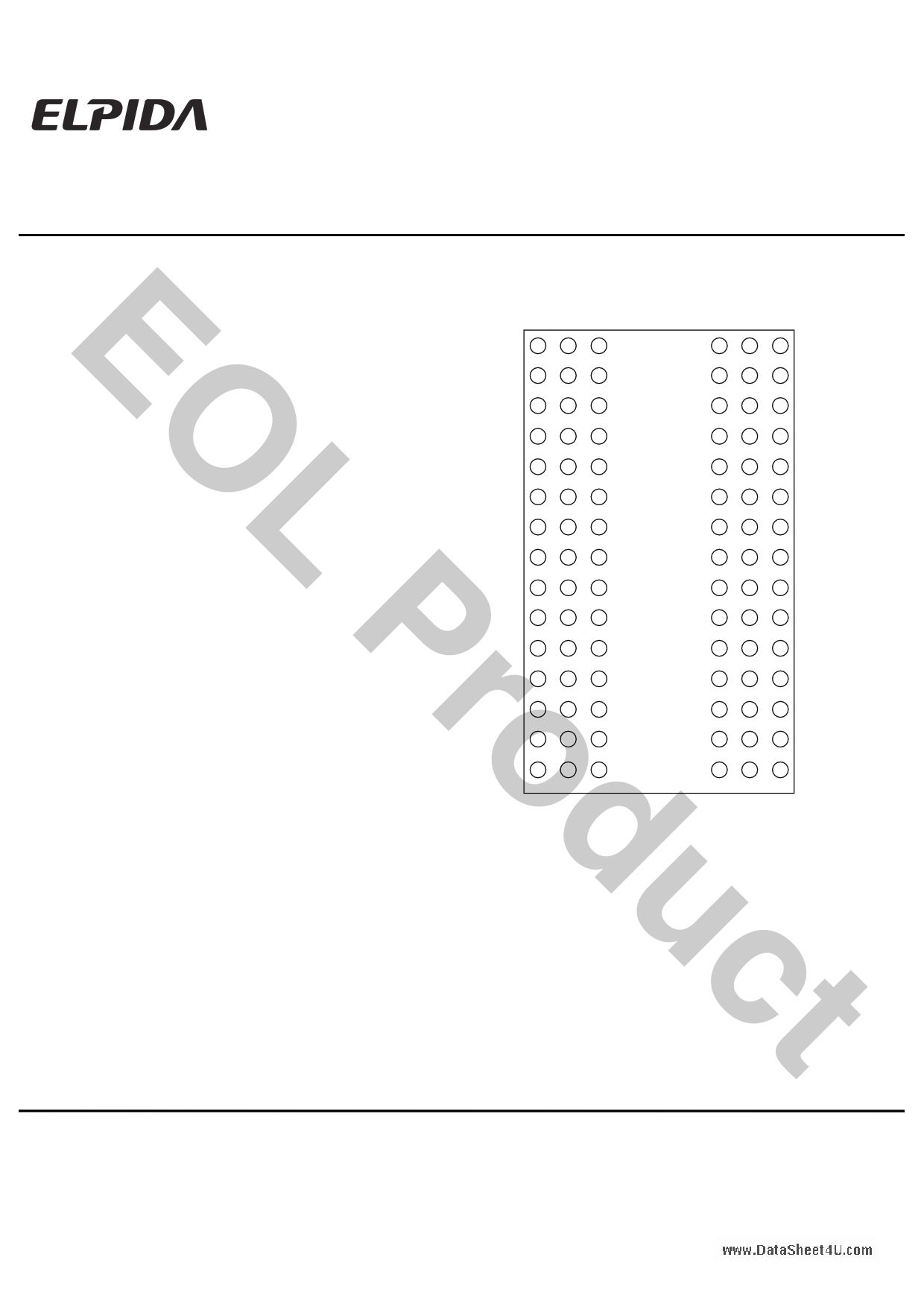
Pin Configurations
/xxx indicates active low signal.
90-ball FBGA
123456789
A
DQ26 DQ24 VSS
B
DQ28 VDDQ VSSQ
C
VSSQ DQ27 DQ25
D
VSSQ DQ29 DQ30
E
VDDQ DQ31 NC
F
VSS DQM3 A3
G
A4 A5 A6
H
A7 A8 NC
J
CLK CKE A9
K
DQM1 NC NC
L
VDDQ DQ8 VSS
M
VSSQ DQ10 DQ9
N
VSSQ DQ12 DQ14
P
DQ11 VDDQ VSSQ
R
DQ13 DQ15 VSS
(Top view)
VDD DQ23 DQ21
VDDQ VSSQ DQ19
DQ22 DQ20 VDDQ
DQ17 DQ18 VDDQ
NC DQ16 VSSQ
A2 DQM2 VDD
A10 A0 A1
NC BA1 A11
BA0 /CS /RAS
/CAS /WE DQM0
VDD DQ7 VSSQ
DQ6 DQ5 VDDQ
DQ1 DQ3 VDDQ
VDDQ VSSQ DQ4
VDD DQ0 DQ2
A0 to A11
BA0, BA1
DQ0 to DQ31
/CS
/RAS
/CAS
/WE
DQM0 to DQM3
CKE
CLK
VDD
VSS
VDDQ
VSSQ
NC
Address inputs
Bank select address
Data-input/output
Chip select
Row address strobe
Column address strobe
Write enable
DQ mask enable
Clock enable
Clock input
Power for internal circuit
Ground for internal circuit
Power for DQ circuit
Ground for DQ circuit
No connection
Document No. E0508E40 (Ver. 4.0)
Date Published December 2005 (K) Japan
Printed in Japan
URL: http://www.elpida.com
This product became EOL in March, 2007.
©Elpida Memory, Inc. 2004-2005
1 page 
EDS2532AABJ-75
www.DataSheet4U.com
DC Characteristics 1 (TA = 0 to +70°C, VDD, VDDQ = 3.3V ± 0.3V, VSS, VSSQ = 0V)
Parameter
/CAS latency
Operating current
Symbol
IDD1
Grade
Standby current in power down
Standby current in power down
(input signal stable)
Standby current in non power down
Standby current in non power down
(input signal stable)
Active standby current in power down
Active standby current in power down
(input signal stable)
Active standby current in non power down
Active standby current in non power down
(input signal stable)
Burst operating current
IDD2P
IDD2PS
IDD2N
IDD2NS
IDD3P
IDD3PS
IDD3N
IDD3NS
IDD4
max.
125
3
2
20
9
4
3
45
30
150
Unit Test condition
mA
Burst length = 1
tRC = tRC (min.)
mA
CKE = VIL,
tCK = tCK (min.)
mA CKE = VIL, tCK = ∞
mA
CKE, /CS = VIH,
tCK = tCK (min.)
mA
CKE = VIH, tCK = ∞,
/CS = VIH
mA
CKE = VIL,
tCK = tCK (min.)
mA CKE = VIL, tCK = ∞
mA
CKE, /CS = VIH,
tCK = tCK (min.)
mA
CKE = VIH, tCK = ∞,
/CS = VIH
mA
tCK = tCK (min.),
BL = 4
Notes
1, 2, 3
6
7
4
8
1, 2, 6
2, 7
1, 2, 4
2, 8
1, 2, 5
Refresh current
IDD5
270 mA tRC = tRC (min.)
3
Self refresh current
IDD6
3
mA
VIH ≥ VDD – 0.2V
VIL ≤ 0.2V
Self refresh current
(L-version)
IDD6
-XXL
1
mA
VIH ≥ VDD – 0.2V
VIL ≤ 0.2V
Notes: 1. IDD depends on output load condition when the device is selected. IDD (max.) is specified at the output
open condition.
2. One bank operation.
3. Input signals are changed once per one clock.
4. Input signals are changed once per two clocks.
5. Input signals are changed once per four clocks.
6. After power down mode, CLK operating current.
7. After power down mode, no CLK operating current.
8. Input signals are VIH or VIL fixed.
Data Sheet E0508E40 (Ver. 4.0)
5
5 Page 
EDS2532AABJ-75
www.DataSheet4U.com
Command Operation
Command Truth Table
The SDRAM recognizes the following commands specified by the /CS, /RAS, /CAS, /WE and address pins.
CKE
Function
Symbol n – 1 n
/CS /RAS /CAS /WE BA1,BA0 A10
Device deselect
No operation
DESL
NOP
H
H
×
×
H×
×
L HH
××
H×
×
×
Burst stop
BST H × L H H L ×
Read
READ
H
×
L
HL
HV
Read with auto precharge
READA H
×
L
HL
HV
Write
WRIT
H
×
L
HL
L
V
Write with auto precharge
WRITA H
×
L
HL
L
V
Bank activate
ACT H × L L H H V
Precharge select bank
PRE H × L L H L V
Precharge all banks
PALL
H
×
L
L
H
L
×
×
L
H
L
H
V
L
H
Mode register set
MRS
H
×
L
L
L
L
L
Remark: H: VIH. L: VIL. ×: VIH or VIL. V: Valid address input.
L
A0 to A11
×
×
×
V
V
V
V
V
×
×
V
Device deselect command [DESL]
When this command is set (/CS is High), the SDRAM ignore command input at the clock. However, the internal
status is held.
No operation [NOP]
This command is not an execution command. However, the internal operations continue.
Burst stop command [BST]
This command can stop the current burst operation.
Column address strobe and read command [READ]
This command starts a read operation. In addition, the start address of burst read is determined by the column
address (see Address Pins Table in Pin Function) and the bank select address (BA0, BA1). After the read operation,
the output buffer becomes High-Z.
Read with auto-precharge [READA]
This command automatically performs a precharge operation after a burst read with a burst length of 1, 2, 4 or 8.
Column address strobe and write command [WRIT]
This command starts a write operation. When the burst write mode is selected, the column address (see Address
Pins Table in Pin Function) and the bank select address (BA0, BA1) become the burst write start address. When the
single write mode is selected, data is only written to the location specified by the column address (see Address Pins
Table in Pin Function) and the bank select address (BA0, BA1).
Write with auto-precharge [WRITA]
This command automatically performs a precharge operation after a burst write with a length of 1, 2, 4 or 8, or after a
single write operation.
Data Sheet E0508E40 (Ver. 4.0)
11
11 Page | ||
| Páginas | Total 48 Páginas | |
| PDF Descargar | [ Datasheet EDS2532AABJ-75.PDF ] | |
Hoja de datos destacado
| Número de pieza | Descripción | Fabricantes |
| EDS2532AABJ-75 | 256M bits SDRAM | Elpida Memory |
| Número de pieza | Descripción | Fabricantes |
| SLA6805M | High Voltage 3 phase Motor Driver IC. |
Sanken |
| SDC1742 | 12- and 14-Bit Hybrid Synchro / Resolver-to-Digital Converters. |
Analog Devices |
|
DataSheet.es es una pagina web que funciona como un repositorio de manuales o hoja de datos de muchos de los productos más populares, |
| DataSheet.es | 2020 | Privacy Policy | Contacto | Buscar |