|
|
|
PDF FSP3129 Data sheet ( Hoja de datos )
| Número de pieza | FSP3129 | |
| Descripción | WIDE INPUT 2A STEP DOWN CONVERTER | |
| Fabricantes | FOSLINK SEMICONDUCTOR | |
| Logotipo | ||
Hay una vista previa y un enlace de descarga de FSP3129 (archivo pdf) en la parte inferior de esta página. Total 10 Páginas | ||
|
No Preview Available !
www.DataSheet4U.com
WIDE INPUT 2A STEP-DOWN CONVERTER
FEATURES
z 2A Output Current
z Up to 95% Efficiency
z Up to 30V Input Range
z 6µA Shutdown Supply Current
z 400kHz Switching Frequency
z Adjustable Output Voltage
z Cycle-by-Cycle Current Limit Protection
z Thermal Shutdown Protection
z Frequency Fold Back at Short Circuit
z Stability with Wide Range of Capacitors,
Including Low ESR Ceramic Capacitors
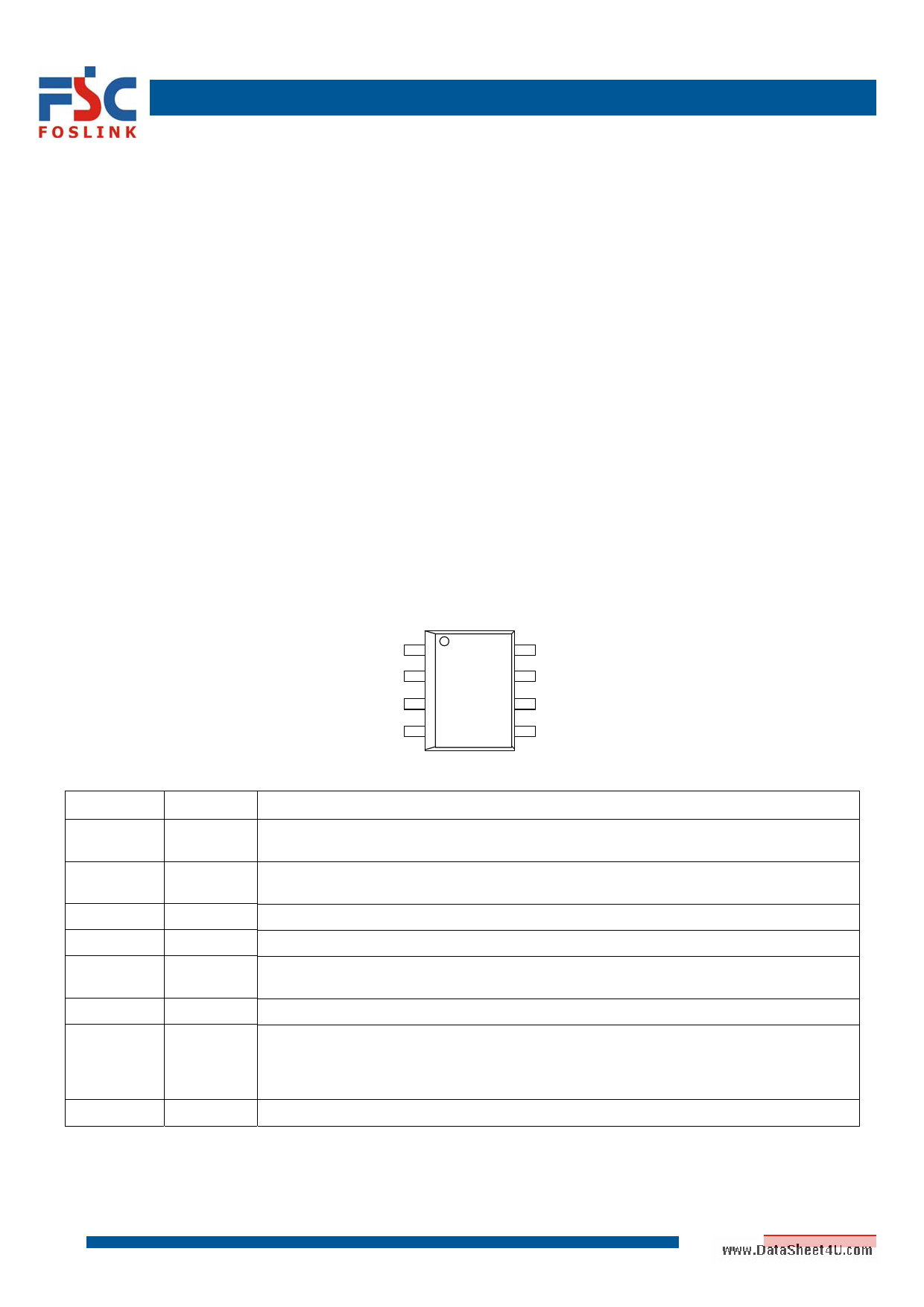
z SOP8L Package
TYPICAL APPLICATION
z TFT LCD Monitors or Televisions and HDTV
z Portable DVD Players
z Car-Powered or Battery-Powered Equipment
z Set-Top Boxes
z Telecom Power Supplies
z DSL and Cable Modems and Routers
FSP3129
GENERAL DESCRIPTION
The FSP3129 is a current-mode step-down DC/DC
converter that generates up to 2A output current at
400kHz switching frequency. The device can
operate with input voltage up to 30V.
Consuming only 6µA in shutdown mode, the
FSP3129 is highly efficient with peak efficiency at
95% when in operation. Protection features include
cycle-by-cycle current limit, thermal shutdown, and
frequency fold back at short circuit.
The FSP3129 is available in SOP8L package and
requires very few external devices for operation.
PIN ASSIGNMENT
(Top View)
BS 1
IN 2
SW 3
G4
8 N/C
7 EN
6 COMP
5 FB
PIN DESCRIPTION
Pin Number Pin Name
Pin Description
1
BS
Bootstrap. This pin acts as the positive rail for the high-side switch’s gate driver.
Connect a 10nF between this pin and SW.
2
IN
Input Supply. Bypass this pin to G with a low ESR capacitor. See Input Capacitor in
Application Information section.
3 SW Switch Output. Connect this pin to the switching end of the inductor.
4 G Ground.
5
FB
Feedback Input. The voltage at this pin is regulated to 1.222V. Connect to the resistor
divider between the output and ground to set output voltage.
6 COMP Compensation Pin. See Compensation Technique in Application information section.
Enable Input. Drive higher than 1.3V or unconnected to enable the IC. Drive lower than
7
EN
0.7V to disable the IC. The IC is in 6µA low current shutdown mode and the output is
discharged through the Low-Side Power Switch. This pin has a small internal pull up
current to a high level voltage when pin is not connected.
8 N/C Not Connected.
1/10 2007-1-4
1 page 
www.DataSheet4U.com
WIDE INPUT 2A STEP-DOWN CONVERTER
FSP3129
Input Capacitor
The input capacitor needs to be carefully selected to maintain sufficiently low ripple at the supply input of the
converter. A low ESR capacitor is highly recommended. Since a large current flows in and out of this capacitor during
switching, its ESR also affects efficiency.
The input capacitance needs to be higher than 10µF. The best choice is the ceramic type, however, low ESR tantalum
or electrolytic types may also be used provided that the RMS ripple current rating is higher than 50% of the output
current. The input capacitor should be placed close to the IN and G pins of the IC, with shortest possible traces. In the
case of tantalum or electrolytic types, they can be further away if a small parallel 0.1µF ceramic capacitor is placed
right next to the IC.
Output Capacitor
The output capacitor also needs to have low ESR to keep low output voltage ripple. The output ripple voltage is:
where IOUTMAX is the maximum output current, KRIPPLE is the ripple factor, RESR is the ESR resistance of the output
capacitor, fSW is the switching frequency, L is the inductor value, COUT is the output capacitance.
In the case of ceramic output capacitors, RESR is very small and does not contribute to the ripple. Therefore, a lower
capacitance value can be used for ceramic type, typically choose a capacitance of about 22µF.
In the case of tantalum or electrolytic type, the ripple is dominated by RESR multiplied by the ripple current. In that case,
the output capacitor is chosen to have sufficiently low due to ESR, typically choose a capacitor with less than 50mΩ
ESR.
Rectifier Diode
Use a Schottky diode as the rectifier to conduct current when the High-Side Power Switch is off. The Schottky diode
must have current rating higher than the maximum output current and the reverse voltage rating higher than the
maximum input voltage.
Stability Compensation
CCOMP2 is needed only for high ESR output capacitor
Figure 2: Stability compensation
The feedback system of the IC is stabilized by the components at COMP pin, as shown in Figure 2. The DC loop gain
of the system is determined by the following equation:
The dominant pole P1 is due to CCOMP
The second pole P2 is the output pole:
The first zero Z1 is due RCOMP and CCOMP
5/10 2007-1-4
5 Page | ||
| Páginas | Total 10 Páginas | |
| PDF Descargar | [ Datasheet FSP3129.PDF ] | |
Hoja de datos destacado
| Número de pieza | Descripción | Fabricantes |
| FSP3122 | 150KHZ 3A PWM BUCK DC/DC CONVERTER | FOSLINK SEMICONDUCTOR |
| FSP3123 | 150KHZ 3A PWM BUCK DC/DC CONVERTER | FOSLINK SEMICONDUCTOR |
| FSP3124 | 150KHZ 3A PWM BUCK DC/DC CONVERTER | FOSLINK SEMICONDUCTOR |
| FSP3125 | 150KHZ 2A PWM BUCK DC/DC CONVERTER | FOSLINK SEMICONDUCTOR |
| Número de pieza | Descripción | Fabricantes |
| SLA6805M | High Voltage 3 phase Motor Driver IC. |
Sanken |
| SDC1742 | 12- and 14-Bit Hybrid Synchro / Resolver-to-Digital Converters. |
Analog Devices |
|
DataSheet.es es una pagina web que funciona como un repositorio de manuales o hoja de datos de muchos de los productos más populares, |
| DataSheet.es | 2020 | Privacy Policy | Contacto | Buscar |