|
|
PDF MAX11201 Data sheet ( Hoja de datos )
| Número de pieza | MAX11201 | |
| Descripción | Delta- Sigma ADC | |
| Fabricantes | Maxim Integrated Products | |
| Logotipo |  |
|
Hay una vista previa y un enlace de descarga de MAX11201 (archivo pdf) en la parte inferior de esta página. Total 14 Páginas | ||
|
No Preview Available !
19-5333; Rev 0; 6/10
EVAALVUAAILTAIOBNLEKIT
www.DataSheet4U.com
24-Bit, Single-Channel, Ultra-Low-Power, Delta
Sigma ADC with 2-Wire Serial Interface
General Description
The MAX11201 is an ultra-low-power (< 320FA max
active current), high-resolution, serial-output ADC. This
device provides the highest resolution per unit power in
the industry and is optimized for applications that require
very high dynamic range with low power such as sensors
on a 4mA to 20mA industrial control loop. The MAX11201
provides a high-accuracy internal oscillator that requires
no external components.
When used with the specified data rates, the internal digital
filter provides more than 100dB rejection of 50Hz or 60Hz
line noise. The MAX11201 provides a simple 2-wire serial
interface in the space-saving, 10-pin FMAXM package.
The MAX11201 operates over the -40NC to +85NC tem-
perature range.
Sensor Measurement
(Temperature and
Pressure)
Applications
Portable Instrumentation
Battery Applications
Weigh Scales
Ordering Information
PART
PIN-PACKAGE
OUTPUT RATE
(sps)
MAX11201AEUB+ 10 FMAX
MAX11201BEUB+ 10 FMAX
120
13.75
Note: All devices are specified over the -40°C to +85°C oper-
ating temperature range.
+Denotes a lead(Pb)-free/RoHS-compliant package.
RESOLUTION
(BITS)
24
20
18
16
4-WIRE SPI, 16-PIN QSOP,
PROGRAMMABLE GAIN
MAX11210
MAX11206
MAX11209
MAX11213
Features
S 23.3-Bit ENOB
20.6-Bit Noise-Free Resolution at 13.75sps
19.1-Bit Noise-Free Resolution at 120sps
S 700nVRMS Noise ±3.6VFS Input (MAX11201B)
S INL: 3ppm (typ), 10ppm (max)
S No Missing Codes
S Ultra-Low Power Dissipation
Operating Mode Current Drain < 320µA (max)
Sleep Mode Current Drain < 0.4µA
S 2.7V to 3.6V Analog Supply Voltage Range
S 1.7V to 3.6V Digital and I/O Supply Voltage Range
S Fully Differential Signal and Reference Inputs
S High-Impedance Inputs
Buffers on Signal Inputs
S Programmable Internal System Clock or External
Clock
2.4576MHz (MAX11201A)
2.25275MHz (MAX11201B)
S > 100dB (min) 50Hz/60Hz Rejection (MAX11201B)
S Serial 2-Wire Interface (Clock Input and Data Output)
S On-Demand Offset and Gain Self-Calibration
S -40°C to +85°C Operating Temperature Range
S ±2kV ESD Protection
S Lead(Pb)-Free and RoHS-Compliant µMAX Package
4-WIRE SPI,
16-PIN QSOP
MAX11200
MAX11207
MAX11211
MAX11203
Selector Guide
2-WIRE SERIAL,
10-PIN μMAX
MAX11201 (with buffers)
MAX11202 (without buffers)
MAX11208
MAX11212
MAX11205
µMAX is a registered trademark of Maxim Integrated Products, Inc.
________________________________________________________________ Maxim Integrated Products 1
For pricing, delivery, and ordering information, please contact Maxim Direct at 1-888-629-4642,
or visit Maxim’s website at www.maxim-ic.com.
1 page 
www.DataSheet4U.com
24-Bit, Single-Channel, Ultra-Low-Power, Delta
Sigma ADC with 2-Wire Serial Interface
Typical Operating Characteristics
(VAVDD = 3.6V, VDVDD = 1.8V, VREFP - VREFN = AVDD; internal clock; TA = TMIN to TMAX, unless otherwise specified. Typical values
are at TA = +25NC.)
ANALOG ACTIVE CURRENT
vs. AVDD VOLTAGE (MAX11201A)
240
ANALOG ACTIVE CURRENT
vs. AVDD VOLTAGE (MAX11201B)
240
ANALOG SLEEP CURRENT
vs. AVDD VOLTAGE
1.0
220 TA = +85°C
200 TA = +25°C
180
220
TA = +85°C
200
TA = +25°C
180
0.8
0.6
160 TA = -45°C
140
120
100
2.70 2.85 3.00 3.15 3.30 3.45 3.60
AVDD VOLTAGE (V)
160 TA = -45°C
140
120
100
2.70 2.85 3.00 3.15 3.30 3.45 3.60
AVDD VOLTAGE (V)
0.4
0.2 TA = +85°C TA = -45°C
TA = +25°C
0
2.7 2.8 2.9 3.0 3.1 3.2 3.3 3.4 3.5 3.6
AVDD VOLTAGE (V)
ACTIVE SUPPLY CURRENT
vs. TEMPERATURE (MAX11201A)
300
250 TOTAL
200 VAVDD = 3.0V
150
100
VDVDD = 1.8V
50
ACTIVE SUPPLY CURRENT
vs. TEMPERATURE (MAX11201B)
300
250 TOTAL
200
VAVDD = 3.0V
150
100
VDVDD = 1.8V
50
SLEEP CURRENT vs. TEMPERATURE
1.0
VAVDD = 3.0V
0.8
0.6
0.4
0.2
AVDD
DVDD TOTAL
0
-45 -25 -5 15 35 55 75 95
TEMPERATURE (°C)
DIGITAL ACTIVE CURRENT
vs. DVDD VOLTAGE
130
TA = +85°C, +25°C, -45°C
120
110
100 MAX11201A
90
80
70 MAX11201B
60
50
40
1.6 1.8 2.0 2.2 2.4 2.6 2.8 3.0 3.2 3.4 3.6
DVDD VOLTAGE (V)
0
-45 -25 -5 15 35 55 75 95
TEMPERATURE (°C)
DIGITAL SLEEP CURRENT
vs. DVDD VOLTAGE
3.0
2.5 TA = -45°C
2.0 TA = +25°C
1.5
1.0 TA = +85°C
0.5
0
1.7 1.9 2.1 2.3 2.5 2.7 2.9 3.1 3.3 3.5
DVDD VOLTAGE (V)
0
-45 -25 -5 15 35 55 75 95
TEMPERATURE (°C)
INTERNAL OSCILLATOR FREQUENCY
vs. TEMPERATURE
2.6
VAVDD = 3.0V
2.5 MAX11201A
2.4
2.3 MAX11201B
2.2
2.1
2.0
-45 -25 -5 15 35 55 75 95
TEMPERATURE (°C)
_______________________________________________________________________________________ 5
5 Page 
www.DataSheet4U.com
24-Bit, Single-Channel, Ultra-Low-Power, Delta
Sigma ADC with 2-Wire Serial Interface
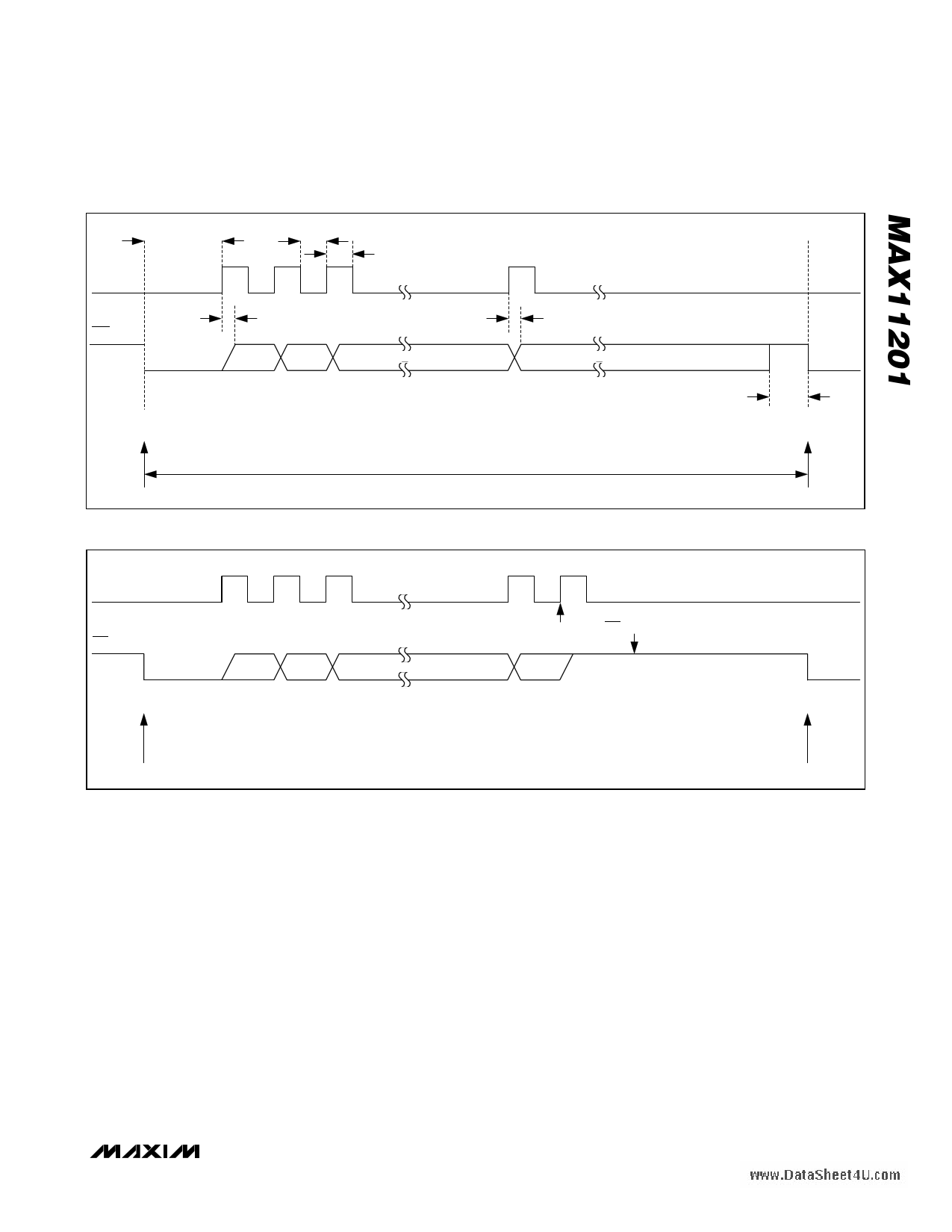
SCLK
RDY/DOUT
t5
1
t3
t1
t2
23
D23 D22
CONVERSION IS DONE
DATA IS AVAILABLE
24
t4
D0
t7
t6
CONVERSION IS DONE
DATA IS AVAILABLE
Figure 1. Timing Diagram for Data Read After Conversion
SCLK
12 3
RDY/DOUT
CONVERSION IS DONE
DATA IS AVAILABLE
D23 D22
24
D0
25
25TH SLK RISING EDGE
PULLS RDY/DOUT
HIGH
CONVERSION IS DONE
DATA IS AVAILABLE
Figure 2. Timing Diagram for Data Read Followed by RDY/DOUT Being Asserted High Using 25th SCLK
Data Read Followed by Self-Calibration
To initiate self-calibration at the end of a data read, pro-
vide a 26th SCLK clock pulse. After reading the 24 bits
of conversion data, a 25th positive edge on SCLK pulls
the RDY/DOUT output back high, indicating the end of
the data read. Provide a 26th SCLK clock pulse to initi-
ate a self-calibration routine starting on the falling edge
of the SCLK. A subsequent falling edge of RDY/DOUT
indicates data availability at the end of calibration. The
timing is illustrated in Figure 3.
Data Read Followed by Sleep Mode
The MAX11201 can be put into sleep mode to save
power between conversions. To activate the sleep mode,
idle the SCLK high any time after the RDY/DOUT output
goes low (that is, after conversion data is available). It is
not required to read out all 24 bits before putting the part
in sleep mode. Sleep mode is activated after the SCLK is
held high (see Figure 4). The RDY/DOUT output is pulled
high once the device enters sleep mode. To come out
of the sleep mode, pull SCLK low. After the sleep mode
is deactivated (when the device wakes up), conversion
starts again and RDY/DOUT goes low, indicating the
next conversion data is available (see Figure 4).
Single-Conversion Mode
For operating the MAX11201 in single-conversion mode,
activate and deactivate sleep mode between conver-
sions as described in the Data Read Followed by Sleep
Mode section). Single-conversion mode reduces power
consumption by shutting down the device when idle
between conversions. See Figure 4.
______________________________________________________________________________________ 11
11 Page | ||
| Páginas | Total 14 Páginas | |
| PDF Descargar | [ Datasheet MAX11201.PDF ] | |
Hoja de datos destacado
| Número de pieza | Descripción | Fabricantes |
| MAX11200 | Delta- Sigma ADCs | Maxim Integrated Products |
| MAX11201 | Delta- Sigma ADC | Maxim Integrated Products |
| MAX11202 | Delta- Sigma ADC with 2-Wire Serial Interface | Maxim Integrated Products |
| MAX11203 | Delta- Sigma ADCs | Maxim Integrated Products |
| Número de pieza | Descripción | Fabricantes |
| SLA6805M | High Voltage 3 phase Motor Driver IC. |
Sanken |
| SDC1742 | 12- and 14-Bit Hybrid Synchro / Resolver-to-Digital Converters. |
Analog Devices |
|
DataSheet.es es una pagina web que funciona como un repositorio de manuales o hoja de datos de muchos de los productos más populares, |
| DataSheet.es | 2020 | Privacy Policy | Contacto | Buscar |
