|
|
|
PDF 78P2351R Data sheet ( Hoja de datos )
| Número de pieza | 78P2351R | |
| Descripción | Serial 155M NRZ to CMI Converter | |
| Fabricantes | Teridian Semiconductor | |
| Logotipo | ||
Hay una vista previa y un enlace de descarga de 78P2351R (archivo pdf) en la parte inferior de esta página. Total 31 Páginas | ||
|
No Preview Available !
DESCRIPTION
The 78P2351R is Teridian’s second generation Line
Interface Unit (LIU) for 155 Mbit/s electrical SDH
interfaces (STM1e). The device is a single chip
solution that includes an integrated Clock & Data
Recovery in both the transmit and receive paths for
easy, cost efficient NRZ to CMI conversion.
The device interfaces to 75Ω coaxial cable through
wideband transformers and can handle over 12.7dB
of cable loss. By eliminating the needs for
synchronous clocks, the small 78P2351R (7x7mm
MLF package) is ideal for new STM1e (ES1) Small
Form-factor Pluggable (SFP) transceiver modules.
APPLICATIONS
• STM1e SFP modules
• SDH/ATM Line Cards
• Add Drop Multiplexers (ADMs)
• PDH/SDH Test Equipment
• Digital Microwave Radios
• Multi-Service Switches
78P2351Rwww.DataSheet4U.com
Serial 155M
NRZ to CMI Converter
DATA SHEET
AUGUST 2006
FEATURES
• ITU-T G.703 compliant, adjustable cable driver
for 155.52 Mbps CMI-coded coax transmission
• Integrated adaptive CMI equalizer and CDR in
receive path handles over 12.7dB of cable loss
• LVPECL-compatible system interface with
integrated CDR in transmit path for flexible NRZ
to CMI conversion
• Configurable via HW control pins or 4-wire serial
port interface
• Compliant with ANSI T1.105.03-1994; ITU-T
G.813, G.825, G.958; and Telcordia GR-253-
CORE for jitter performance
• Receive Loss of Signal (Rx LOS) detection
• Receive Monitor Mode handles up to 20dB of
flat loss (at max 6dB cable loss)
• Optional fixed backplane equalizer compensates
for up to 1.5m of trace
• Operates from a single 3.3V supply
• Available in a small 7x7mm 56-pin QFN
package
• Industrial Temperature: -40˚C to +85˚C
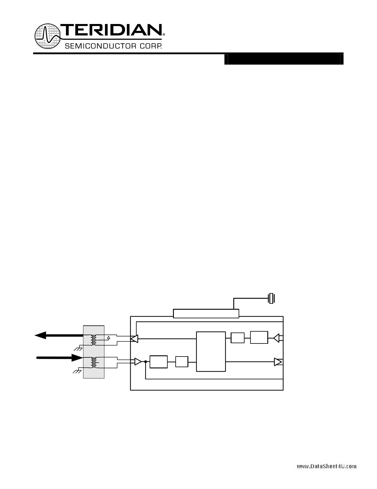
BLOCK DIAGRAM
75ohm Coax
(CMI Encoded)
78P2351R
Adaptive
Eq.
CDR
CDR
Fixed
Eq.
CMI
ENDEC
Tx Disable
TD +
TD -
RD +
RD -
LVPECL Data
(NRZ Encoded)
Rx LOS
Page: 1 of 31
2006 Teridian Semiconductor Corporation
Rev. 2.1
1 page 
TRANSMITTER OPERATION
The transmitter section generates an adjustable
ITU-T G.703 compliant analog signal for
transmission through a wideband transformer onto
75Ω coaxial cable. Differential NRZ data is input to
the 78P2351R on the SIDP/N pins at LVPECL levels
and passed to a low jitter clock and data recovery
circuit. An optional clock decoupling FIFO is
provided to decouple the on chip and off chip clocks.
The NRZ data is encoded using CMI line coding to
ensure an adequate number of transitions.
Each of the transmit timing modes can be configured
in HW mode or SW mode as shown in the table
below.
Tx Mode
HW Control
CKMODE
SW Control
SMOD[1:0]
Reserved
Low
00
Synchronous
(FIFO enabled)
Floating
10
Plesiochronous
High
01
Loop-timing
n/a
11
Plesiochronous Mode
Plesiochronous mode represents a common
condition where a synchronous reference clock is
not available. In this mode, the 78P2351R will
recover the transmit clock from the plesiochronous
data and bypass the internal FIFO and re-timing
block. This mode is commonly used for mezzanine
cards, modules, and any application where the
reference clock can’t always be synchronous to the
transmit source clock/data
System
Clock
XO
Framer/
Mapper
NRZ
NRZ
CKREFP
SIDP/N
SODP/N
TDK
78P2351R
CMI Coax
CMIP/N
XFMR
CMI Coax
RXP/N
XFMR
Figure 1: Plesiochronous Mode
www7.D8atPaS2he3et54U1.cRom
Serial 155M
NRZ to CMI Converter
Synchronous Mode
When the NRZ transmit data is source synchronous
with the reference clock applied at CKREFP/N as
shown in Figure 2, the 78P2351R can be optionally
used in synchronous mode or re-timing mode. In
this mode, the 78P2351R will recover the clock from
the NRZ data input and re-time the data in an
integrated +/- 4-bit FIFO.
System Reference Clock
Framer/
Mapper
NRZ
NRZ
CKREFP/N
SIDP/N
SODP/N
TDK
78P2351R
CMI Coax
CMIP/N
XFMR
CMI Coax
RXP/N
XFMR
Figure 2: Synchronous
Since the reference clock and transmit clock/data go
through different delay paths, it is inevitable that the
phase relationship between the two clocks can vary
in a bounded manner due to the fact that the
absolute delays in the two paths can vary over time.
The transmit FIFO allows long-term clock phase drift
between the Tx clock and system reference clock,
not exceeding +/- 25.6ns, to be handled without
transmit error. If the clock wander exceeds the
specified limits, the FIFO will over or under flow, and
the FERR register signal will be asserted. This
signal can be used to trigger an interrupt. This
interrupt event is automatically cleared when a FIFO
Reset (FRST) pulse is applied, and the FIFO is re-
centered.
Notes:
1) External remote loopbacks (i.e. loopback
within framer) are not possible in
synchronous operation (FIFO enabled)
unless the data is re-justified to be
synchronous to the system reference clock
or the 78P2351R is configured for loop-
timing operation.
2) During IC power-up or transmit power-up,
the clocks going to the FIFO may not be
stable and cause the FIFO to overflow or
underflow. As such, the FIFO should be
manually reset using FRST anytime the
transmitter is powered-up.
Clock Synthesizer
The transmit clock synthesizer is a low-jitter PLL that
generates a 311.04 MHz clock for the CMI encoder.
A synthesized 155.52 MHz reference clock is also
used in both the receive and transmit sides for clock
and data recovery.
Page: 5 of 31
2006 Teridian Semiconductor Corporation
Rev. 2.1
5 Page 
www7.D8atPaS2he3et54U1.cRom
Serial 155M
NRZ to CMI Converter
REGISTER DESCRIPTION (continued)
ADDRESS 1-1: SIGNAL CONTROL REGISTER
BIT
NAME
TYPE
DFLT
VALUE
DESCRIPTION
Transmit CMI Inversion:
7 TCMIINV R/W
This bit will flip the polarity of the transmit CMI data outputs at CMIP/N.
0 For debug use only.
0: Normal
1: Invert
Receive CMI Inversion:
6 RCMIINV R/W
This bit will flip the polarity of the receive CMI data inputs at RXP/N. For
0 debug use only.
0: Normal
1: Invert
Receive Loss of Signal Override/Disable:
5 LOSOR R/W
0
When set, the LOS signal will always remain low.
0: Normal
1: Forces LOS output to be low and resets counter
Analog Loopback Selection:
4 RLBK R/W
0 RLBK LLBK
0 0 Normal operation
1 0 Remote Loopback Enable: Recovered receive data
is looped back to the transmit driver for retransmission.
3 LLBK R/W
0
0 1 Local Loopback Enable: The transmit data is
looped back and used as the input to the receiver.
2:1 --
R/W
0 FRST R/W
00 Reserved.
FIFO Reset:
0: Normal operation
1: Reset FIFO pointers to default locations.
0 This reset should be initiated anytime the transmitter or IC powers up to
ensure the FIFO is centered after internal VCO clocks and external
transmit clocks are stable.
NOTE: FIFO reset not required for Plesiochronous Mode
ADDRESS 1-2: ADVANCED TRANSMIT CONTROL REGISTER 1
BIT
NAME
TYPE
DFLT
VALUE
DESCRIPTION
7:1 --
R/W
000000
0
Reserved.
0 TXEQ R/W
Transmit Fixed Equalizer Enable:
When enabled, compensates for between 0.75m and 1.5m of FR4 trace
0 to the LVPECL data inputs SIDP/N
0: Normal Operation
1: Enable equalizer
Page: 11 of 31
2006 Teridian Semiconductor Corporation
Rev. 2.1
11 Page | ||
| Páginas | Total 31 Páginas | |
| PDF Descargar | [ Datasheet 78P2351R.PDF ] | |
Hoja de datos destacado
| Número de pieza | Descripción | Fabricantes |
| 78P2351 | Single Channel OC-3/ STM1-E/ E4 LIU | TDK Semiconductor |
| 78P2351R | Serial 155M NRZ to CMI Converter | Teridian Semiconductor |
| Número de pieza | Descripción | Fabricantes |
| SLA6805M | High Voltage 3 phase Motor Driver IC. |
Sanken |
| SDC1742 | 12- and 14-Bit Hybrid Synchro / Resolver-to-Digital Converters. |
Analog Devices |
|
DataSheet.es es una pagina web que funciona como un repositorio de manuales o hoja de datos de muchos de los productos más populares, |
| DataSheet.es | 2020 | Privacy Policy | Contacto | Buscar |