|
|
PDF 25LC512 Data sheet ( Hoja de datos )
| Número de pieza | 25LC512 | |
| Descripción | EEPROM | |
| Fabricantes | Microchip Technology | |
| Logotipo |  |
|
Hay una vista previa y un enlace de descarga de 25LC512 (archivo pdf) en la parte inferior de esta página. Total 30 Páginas | ||
|
No Preview Available !
25LC512
512 Kbit SPI Bus Serial EEPROM
Extended (M) Operating Temperatures
Device Selection Table
Part Number
25LC512
VCC Range
2.5-5.5V
Page Size
128 Byte
Features:
• 10 MHz max. Clock Speed
• Byte and Page-level Write Operations:
- 128-byte page
- 5 ms max.
- No page or sector erase required
• Low-Power CMOS Technology:
- Max. Write Current: 7 mA at 5.5V
- Read Current: 10 mA at 5.5V, 10 MHz
- Standby Current: 1 A at 2.5V, 85°C (Deep
power-down)
• Electronic Signature for Device ID
• Self-Timed Erase and Write Cycles:
- Page Erase (5 ms, typical)
- Sector Erase (10 ms/sector, typical)
- Bulk Erase (10 ms, typical)
• Sector Write Protection (16K byte/sector):
- Protect none, 1/4, 1/2 or all of array
• Built-In Write Protection:
- Power-on/off data protection circuitry
- Write enable latch
- Write-protect pin
• High Reliability:
- Endurance: 1 Million erase/write cycles
- Data Retention: >200 years
- ESD Protection: >4000V
• Temperature Ranges Supported:
- Extended (M):
-55C to +125C
• RoHS Compliant
Pin Function Table
Name
Function
CS
SO
WP
VSS
SI
SCK
HOLD
VCC
Chip Select Input
Serial Data Output
Write-Protect
Ground
Serial Data Input
Serial Clock Input
Hold Input
Supply Voltage
Temp. Ranges
-55°C to +125°C (M)
Packages
SN
Description:
The Microchip Technology Inc. 25LC512 is a 512 Kbit
serial EEPROM memory with byte-level and page-level
serial EEPROM functions. It also features Page, Sector
and Chip erase functions typically associated with
Flash-based products. These functions are not required
for byte or page write operations. The memory is
accessed via a simple Serial Peripheral Interface (SPI)
compatible serial bus. The bus signals required are a
clock input (SCK) plus separate data in (SI) and data out
(SO) lines. Access to the device is controlled by a Chip
Select (CS) input.
Communication to the device can be paused via the
hold pin (HOLD). While the device is paused, transi-
tions on its inputs will be ignored, with the exception of
Chip Select, allowing the host to service higher priority
interrupts.
The 25LC512 is available in the 8-lead SOIC package.
Package Types (not to scale)
SOIC
(SN)
CS 1
SO 2
WP 3
VSS 4
8 VCC
7 HOLD
6 SCK
5 SI
2014 Microchip Technology Inc.
DS20005265A-page 1
1 page 
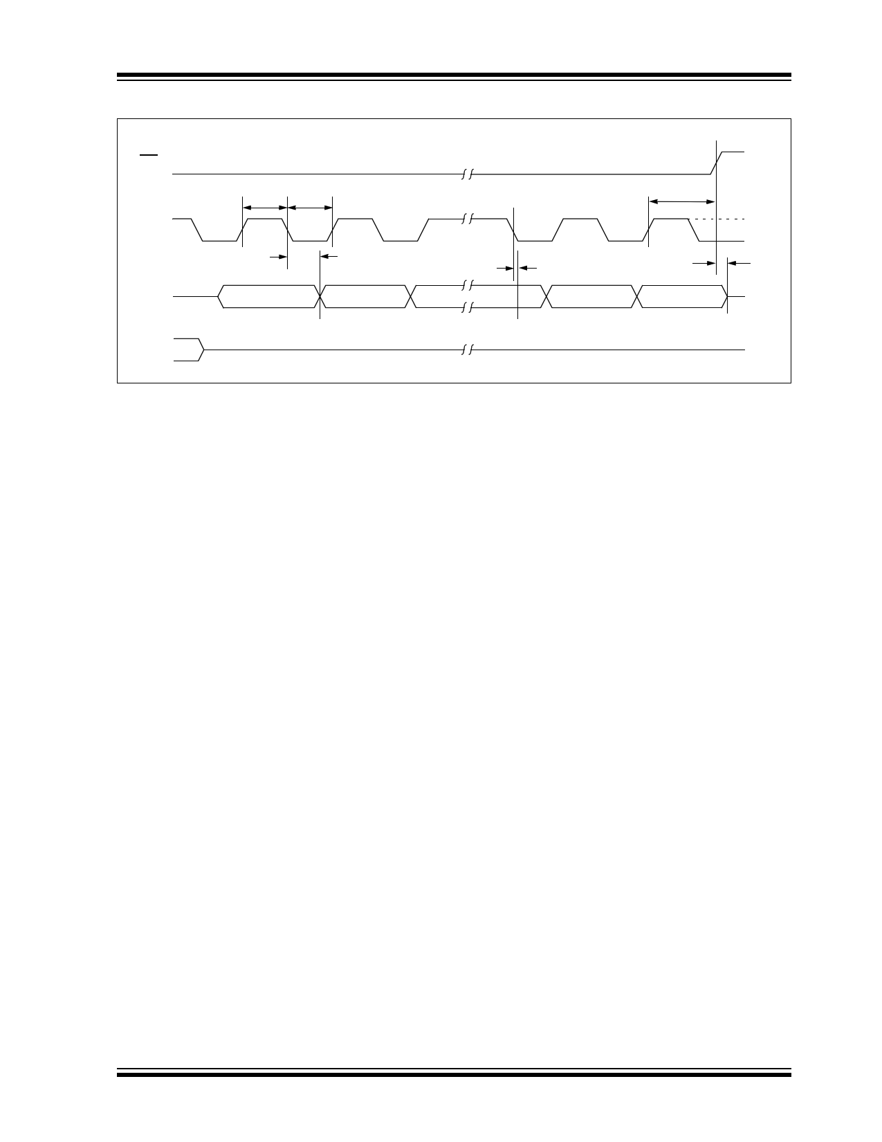
FIGURE 1-3: SERIAL OUTPUT TIMING
CS
SCK
SO
SI
9 10
13
MSB out
Don’t Care
14
25LC512
3
Mode 1,1
Mode 0,0
15
LSB out
2014 Microchip Technology Inc.
DS20005265A-page 5
5 Page 
25LC512
2.4 Read Status Register Instruction
(RDSR)
The Read Status Register instruction (RDSR) provides
access to the STATUS register. The STATUS register
may be read at any time, even during a write cycle. The
STATUS register is formatted as follows:
TABLE 2-2: STATUS REGISTER
7 654 3 2 1
W/R – – – W/R W/R R
WPEN X X X BP1 BP0 WEL
W/R = writable/readable. R = read-only.
0
R
WIP
The Write-In-Process (WIP) bit indicates whether the
25LC512 is busy with a write operation. When set to a
‘1’, a write is in progress, when set to a ‘0’, no write is
in progress. This bit is read-only.
The Write Enable Latch (WEL) bit indicates the status
of the write enable latch and is read-only. When set to
a ‘1’, the latch allows writes to the array, when set to a
‘0’, the latch prohibits writes to the array. The state of
this bit can always be updated via the WREN or WRDI
commands regardless of the state of write protection
on the STATUS register. These commands are shown
in Figure 2-4 and Figure 2-5.
The Block Protection (BP0 and BP1) bits indicate
which blocks are currently write-protected. These bits
are set by the user issuing the WRSR instruction. These
bits are nonvolatile, and are shown in Table 2-3.
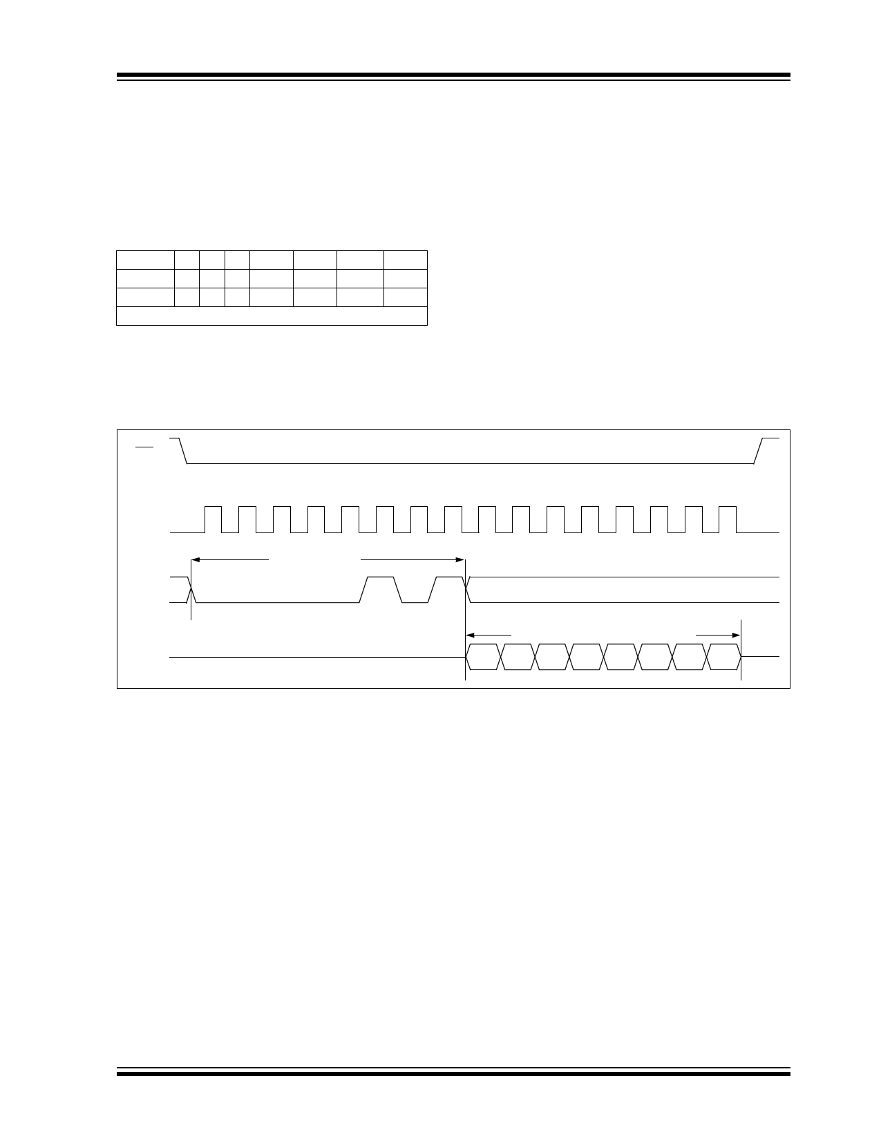
See Figure 2-6 for the RDSR timing sequence.
FIGURE 2-6:
READ STATUS REGISTER TIMING SEQUENCE (RDSR)
CS
SCK
SI
SO
0 1 2 3 4 5 6 7 8 9 10 11 12 13 14 15
Instruction
0 00 00 1 01
High-Impedance
Data from STATUS Register
7 6 54 3 2 10
2014 Microchip Technology Inc.
DS20005265A-page 11
11 Page | ||
| Páginas | Total 30 Páginas | |
| PDF Descargar | [ Datasheet 25LC512.PDF ] | |
Hoja de datos destacado
| Número de pieza | Descripción | Fabricantes |
| 25LC512 | EEPROM | Microchip Technology |
| Número de pieza | Descripción | Fabricantes |
| SLA6805M | High Voltage 3 phase Motor Driver IC. |
Sanken |
| SDC1742 | 12- and 14-Bit Hybrid Synchro / Resolver-to-Digital Converters. |
Analog Devices |
|
DataSheet.es es una pagina web que funciona como un repositorio de manuales o hoja de datos de muchos de los productos más populares, |
| DataSheet.es | 2020 | Privacy Policy | Contacto | Buscar |
