|
|
|
PDF ADT7320 Data sheet ( Hoja de datos )
| Número de pieza | ADT7320 | |
| Descripción | 16-Bit Digital SPI Temperature Sensor | |
| Fabricantes | Analog Devices | |
| Logotipo | ||
Hay una vista previa y un enlace de descarga de ADT7320 (archivo pdf) en la parte inferior de esta página. Total 24 Páginas | ||
|
No Preview Available !
Preliminary Technical Data
FEATURES
Temperature accuracy ±0.25°C from −20°C to +105°C
13- or 16-bit user-selectable temperature-to-digital
converter
Low drift silicon temperature sensor
No temperature calibration/correction required by user
Power saving 1 sample per second (SPS) mode
Fast first conversion on power-up of 6 ms
SPI-compatible interface
Operating temperature from −40°C to +150°C
Operating voltage: 2.7 V to 5.5 V
Critical overtemperature indicator
Programmable overtemperature/undertemperature interrupt
Low power consumption: 700 μW typical at 3.3 V
Shutdown mode for lower power: 7 μW typical at 3.3 V
16-lead RoHS-compliant LFCSP package
APPLICATIONS
RTD and thermistor replacement
Medical equipment
Cold junction compensation
Industrial controls and test
Food transportation and storage
Environmental monitoring and HVAC
±0.25°C Accurate, 16-Bitwww.DataSheet4U.com
Digital SPI Temperature Sensor
ADT7320
GENERAL DESCRIPTION
The ADT7320 is a high accuracy digital temperature sensor
offering breakthrough performance over a wide industrial range,
housed in an LFCSP package. It contains a band gap temperature
reference and a 13-bit analog-to-digital converter (ADC) to
monitor and digitize the temperature to a 0.0625°C resolution.
The ADC resolution, by default, is set to 13 bits (0.0625°C).
This can be changed to 16 bits (0.0078°C) by setting Bit 7 in the
configuration register (Register Address 0x01).
The ADT7320 is guaranteed to operate over supply voltages from
2.7 V to 5.5 V. Operating at 3.3 V, the average supply current is
typically 210 μA. The ADT7320 has a shutdown mode that
powers down the device and offers a shutdown current of
typically 2 μA. The ADT7320 is rated for operation over the
−40°C to +150°C temperature range.
The CT pin is an open-drain output that becomes active when
the temperature exceeds a programmable critical temperature
limit. The default critical temperature limit is 147°C. The INT
pin is also an open-drain output that becomes active when the
temperature exceeds a programmable limit. The INT and CT
pins can operate in either comparator or interrupt mode.
SCLK 1
DOUT 2
DIN 3
CS 4
TEMPERATURE
VALUE
REGISTER
THYST
REGISTER
THIGH
REGISTER
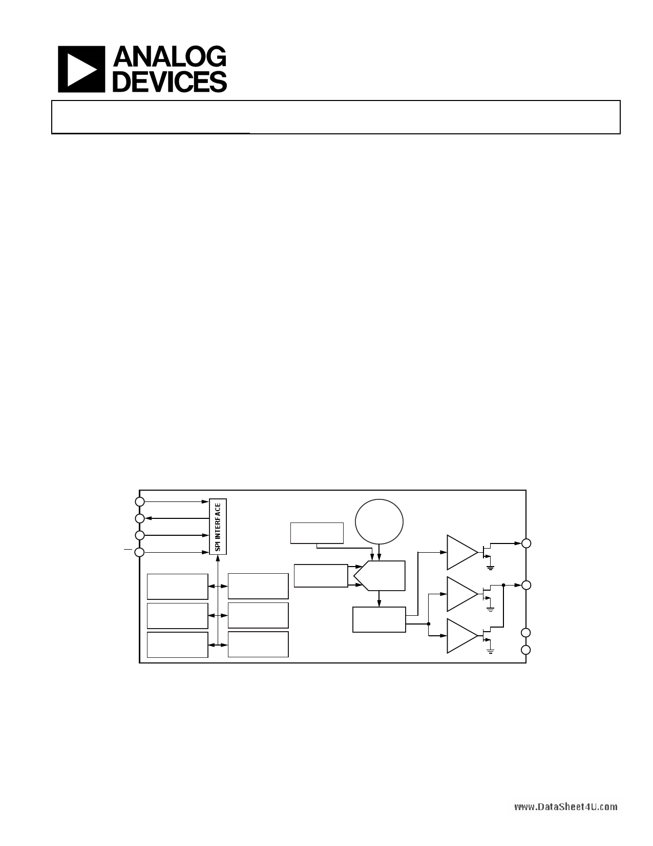
FUNCTIONAL BLOCK DIAGRAM
INTERNAL
REFERENCE
INTERNAL
OSCILLATOR
CONFIGURATION
AND STATUS
REGISTERS
TEMPERATURE
SENSOR
TCRIT
REGISTER
TLOW
REGISTER
Σ-Δ
MODULATOR
FILTER
LOGIC
Figure 1.
ADT7320
TCRIT
THIGH
6 CT
5 INT
TLOW
7 GND
8 VDD
Rev. PrA
Information furnished by Analog Devices is believed to be accurate and reliable. However, no
responsibility is assumed by Analog Devices for its use, nor for any infringements of patents or other
rights of third parties that may result from its use. Specifications subject to change without notice. No
license is granted by implication or otherwise under any patent or patent rights of Analog Devices.
Trademarksandregisteredtrademarksarethepropertyoftheirrespectiveowners.
One Technology Way, P.O. Box 9106, Norwood, MA 02062-9106, U.S.A.
Tel: 781.329.4700
www.analog.com
Fax: 781.461.3113
©2010 Analog Devices, Inc. All rights reserved.
1 page 
Preliminary Technical Data
ABSOLUTE MAXIMUM RATINGS
Table 3.
Parameter
VDD to GND
DIN Input Voltage to GND
DOUT Voltage to GND
SCLK Input Voltage to GND
CS Input Voltage to GND
CT and INT Output Voltage to GND
ESD Rating (Human Body Model)
Operating Temperature Range
Storage Temperature Range
Maximum Junction Temperature, TJMAX
16-Lead LFCSP
Power Dissipation1
Thermal Impedance3
θJA, Junction-to-Ambient (Still Air)
θJC, Junction-to-Case
IR Reflow Soldering
Peak Temperature (RoHS-
Compliant Package)
Time at Peak Temperature
Ramp-Up Rate
Ramp-Down Rate
Time from 25°C to Peak Temperature
Rating
−0.3 V to +7 V
−0.3 V to VDD + 0.3 V
−0.3 V to VDD + 0.3 V
−0.3 V to VDD + 0.3 V
−0.3 V to VDD + 0.3 V
−0.3 V to VDD + 0.3 V
2.0 kV
−40°C to +150°C
−65°C to +160°C
150°C
WMAX = (TJMAX − TA2)/θJA
121°C/W
56°C/W
220°C
260°C (0°C)
20 sec to 40 sec
3°C/sec maximum
−6°C/sec maximum
8 minutes maximum
1 Values relate to package being used on a standard 2-layer PCB. This gives a
worst-case θJA and θJC.
2 TA = ambient temperature.
3 Junction-to-case resistance is applicable to components featuring a
preferential flow direction, for example, components mounted on a heat
sink. Junction-to-ambient is more useful for air-cooled, PCB-mounted
components.
ADT7320www.DataSheet4U.com
Stresses above those listed under Absolute Maximum Ratings
may cause permanent damage to the device. This is a stress
rating only; functional operation of the device at these or any
other conditions above those indicated in the operational
section of this specification is not implied. Exposure to absolute
maximum rating conditions for extended periods may affect
device reliability.
ESD CAUTION
Rev. PrA | Page 5 of 24
5 Page 
Preliminary Technical Data
CT and INT Operation in One-Shot Mode
See Figure 13 for more information on one-shot CT pin
operation for TCRIT overtemperature events when one of the
limits is exceeded. Note that in interrupt mode, a read from
any register resets the INT and CT pins.
For the INT pin in comparator mode, if the temperature drops
below the THIGH − THYST value or goes above the TLOW + THYST
value, a write to the one-shot bits (Bit 5 and Bit 6 of the
configuration register, Register Address 0x01) resets the INT pin.
ADT7320www.DataSheet4U.com
For the CT pin in the comparator mode, if the temperature drops
below the TCRIT − THYST value, a write to the one-shot bits (Bit 5
and Bit 6 of the configuration register, Register Address 0x01)
resets the CT pin, see Figure 13.
Note that when using one-shot mode, ensure that the refresh
rate is appropriate to the application being used.
TEMPERATURE
149°C
148°C
147°C
146°C
145°C
144°C
143°C
142°C
141°C
140°C
CT PIN
POLARITY = ACTIVE LOW
TCRIT
TCRIT – THYST
CT PIN
POLARITY = ACTIVE HIGH
TIME
WRITE TO
BIT 5 AND BIT 6 OF
CONFIGURATION
REGISTER.*
WRITE TO
BIT 5 AND BIT 6 OF
CONFIGURATION
REGISTER.*
WRITE TO
BIT 5 AND BIT 6 OF
CONFIGURATION
REGISTER.*
*THERE IS A 240ms DELAY BETWEEN WRITING TO THE CONFIGURATION REGISTER TO START
A STANDARD ONE-SHOT CONVERSION AND THE CT PIN GOING ACTIVE. THIS IS DUE TO THE
CONVERSION TIME. THE DELAY IS 60ms IN THE CASE OF A ONE-SHOT CONVERSION.
Figure 13. One-Shot CT Pin
Rev. PrA | Page 11 of 24
11 Page | ||
| Páginas | Total 24 Páginas | |
| PDF Descargar | [ Datasheet ADT7320.PDF ] | |
Hoja de datos destacado
| Número de pieza | Descripción | Fabricantes |
| ADT7320 | 16-Bit Digital SPI Temperature Sensor | Analog Devices |
| Número de pieza | Descripción | Fabricantes |
| SLA6805M | High Voltage 3 phase Motor Driver IC. |
Sanken |
| SDC1742 | 12- and 14-Bit Hybrid Synchro / Resolver-to-Digital Converters. |
Analog Devices |
|
DataSheet.es es una pagina web que funciona como un repositorio de manuales o hoja de datos de muchos de los productos más populares, |
| DataSheet.es | 2020 | Privacy Policy | Contacto | Buscar |