|
|
|
PDF ADP8861 Data sheet ( Hoja de datos )
| Número de pieza | ADP8861 | |
| Descripción | 7-Channel Smart LED Driver | |
| Fabricantes | Analog Devices | |
| Logotipo | ||
Hay una vista previa y un enlace de descarga de ADP8861 (archivo pdf) en la parte inferior de esta página. Total 30 Páginas | ||
|
No Preview Available !
Charge Pump, 7-Channelwww.DataSheet4U.com
Smart LED Driver with I2C Interface
ADP8861
FEATURES
Charge pump with automatic gain selection of 1×, 1.5×, and
2× for maximum efficiency
7 independent, programmable LED drivers
7 drivers capable of 30 mA (typical)
1 driver also capable of 60 mA (typical)
Programmable maximum current limit (128 levels)
Standby mode for <1 μA current consumption
16 programmable fade in and fade out times
0.1 sec to 5.5 sec
Choose from linear, square, or cubic rates
Fading override
I2C-compatible interface for all programming
Dedicated reset pin and built-in power-on reset (POR)
Short-circuit, overvoltage, and overtemperature protection
Internal soft start to limit inrush currents
Input-to-output isolation during faults or shutdown
Operation down to VIN = 2.5 V with undervoltage lockout
(UVLO) at VIN = 2.0 V
Small lead frame chip scale package (LFCSP)
APPLICATIONS
Mobile display backlighting
Mobile phone keypad backlighting
Dual RGB backlighting
LED indication
General backlighting of small format displays
GENERAL DESCRIPTION
The ADP8861 provides a powerful charge pump driver with
independent control of up to seven LEDs. These seven LEDs
can be independently driven up to 30 mA (typical). The seventh
LED can also be driven to 60 mA (typical). All LEDs are pro-
grammable for maximum current and fade in/out times via
the I2C interface. These LEDs can also be combined into groups to
reduce the processor instructions during fade in/out.
This entire configuration is driven by a two-capacitor charge
pump with gains of 1×, 1.5×, and 2×. The charge pump is
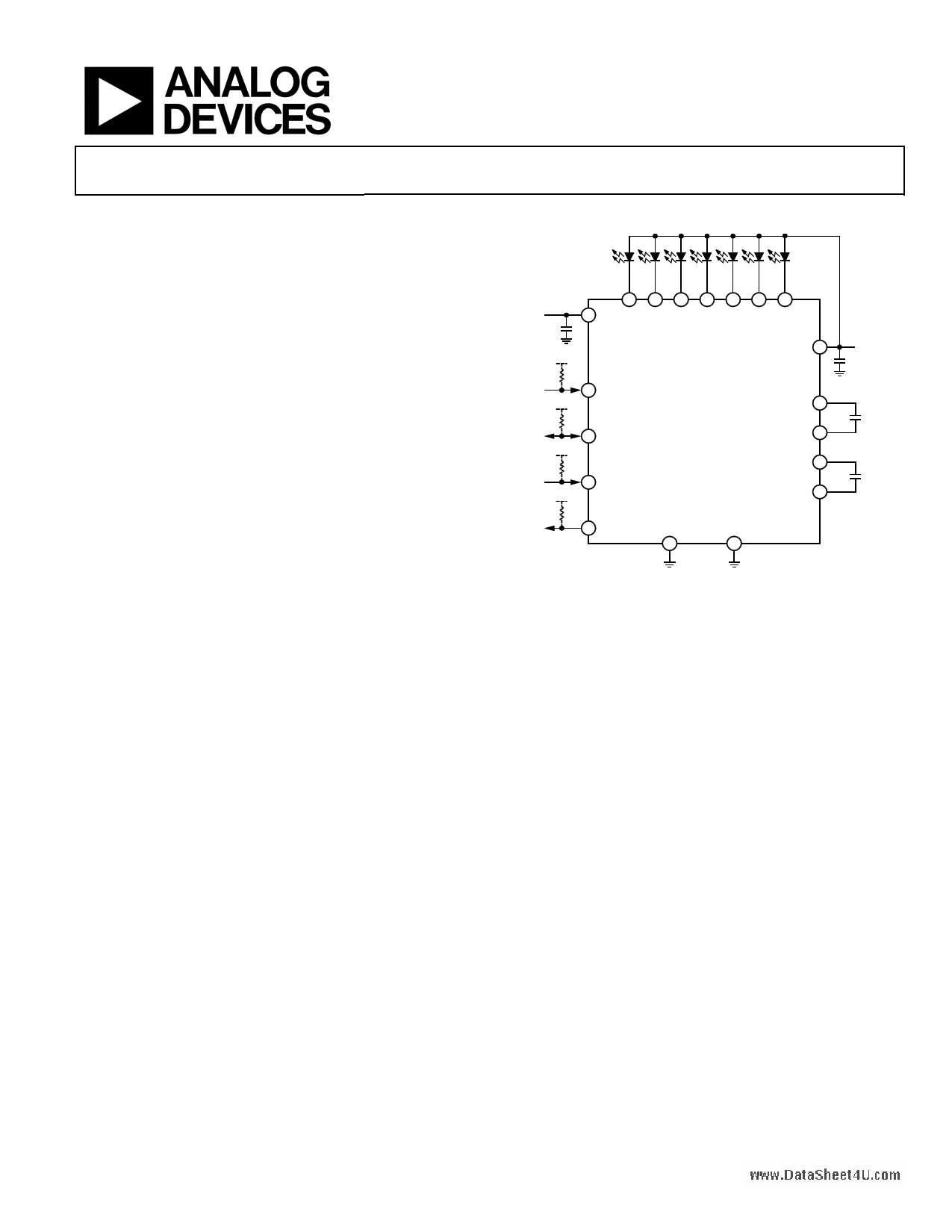
TYPICAL OPERATING CIRCUIT
VIN
CIN
1µF
VDDIO
nRST
VDDIO
SDA
VDDIO
SCL
VDDIO
nINT
D1 D2 D3 D4 D5 D6 D7
ADP8861
GND1
GND2
Figure 1.
VOUT
COUT
1µF
C1+
C1
C1– 1µF
C2+
C2
C2– 1µF
capable of driving a maximum IOUT of 240 mA from a supply
of 2.5 V to 5.5 V. A full suite of safety features, including short-
circuit, overvoltage, and overtemperature protection, allows
easy implementation of a safe and robust design. Additionally,
input inrush currents are limited via an integrated soft start
combined with controlled input-to-output isolation.
The ADP8861 is available in a compact lead frame chip scale
package (LFCSP).
Rev. 0
Information furnished by Analog Devices is believed to be accurate and reliable. However, no
responsibility is assumed by Analog Devices for its use, nor for any infringements of patents or other
rights of third parties that may result from its use. Specifications subject to change without notice. No
license is granted by implication or otherwise under any patent or patent rights of Analog Devices.
Trademarksandregisteredtrademarksarethepropertyoftheirrespectiveowners.
One Technology Way, P.O. Box 9106, Norwood, MA 02062-9106, U.S.A.
Tel: 781.329.4700
www.analog.com
Fax: 781.461.3113
©2010 Analog Devices, Inc. All rights reserved.
1 page 
ABSOLUTE MAXIMUM RATINGS
Table 2.
Parameter
VIN, VOUT
D1, D2, D3, D4, D5, D6, and D7
nINT, nRST, SCL, and SDA
Output Short-Circuit Duration
Operating Temperature Range
Ambient (TA)
Junction (TJ)
Storage Temperature Range
Soldering Conditions
ESD (Electrostatic Discharge)
Human Body Model (HBM)
Charged Device Model (CDM)
Rating
−0.3 V to +6 V
−0.3 V to +6 V
−0.3 V to +6 V
Indefinite
–40°C to +85°C1
–40°C to +125°C
–65°C to +150°C
JEDEC J-STD-020
±3 kV
±1.5 kV
1 The maximum operating junction temperature (TJ(MAX)) takes precedence
over the maximum operating ambient temperature (TA(MAX)). See the
Maximum Temperature Ranges section for more information.
Stresses above those listed under Absolute Maximum Ratings
may cause permanent damage to the device. This is a stress
rating only; functional operation of the device at these or any
other conditions above those indicated in the operational
section of this specification is not implied. Exposure to absolute
maximum rating conditions for extended periods may affect
device reliability.
Absolute maximum ratings apply individually only, not in
combination. Unless otherwise specified, all voltages are
referenced to ground.
ADP8861www.DataSheet4U.com
MAXIMUM TEMPERATURE RANGES
The maximum operating junction temperature (TJ(MAX)) takes
precedence over the maximum operating ambient temperature
(TA(MAX)). Therefore, in situations where the ADP8861 is
exposed to poor thermal resistance and high power dissipation
(PD), the maximum ambient temperature may need to be
derated. In these cases, the maximum ambient temperature can
be calculated with the following equation:
TA(MAX) = TJ(MAX) − (θJA × PD(MAX))
THERMAL RESISTANCE
θJA (junction to air) is specified for the worst-case conditions,
that is, a device soldered in a circuit board for surface-mount
packages. The θJA and θJC (junction to case) are determined
according to JESD51-9 on a 4-layer printed circuit board (PCB)
with natural convection cooling. For the LFCSP package, the
exposed pad must be soldered to the GND1 and/or GND2
terminal on the board.
Table 3. Thermal Resistance
Package Type
20-Lead LFCSP_WQ
θJA
49.5
θJC Unit
5.3 °C/W
ESD CAUTION
Rev. 0 | Page 5 of 40
5 Page 
THEORY OF OPERATION
The ADP8861 provides a powerful charge pump driver with
programmable LED control. Up to seven LEDs can be indepen-
dently driven up to 30 mA (typical) each. The seventh LED can
also be driven to 60 mA (typical). All LEDs can be individually
programmed or combined into a group to operate backlight
ADP8861www.DataSheet4U.com
LEDs. A full suite of safety features, including short-circuit,
overvoltage, and overtemperature protection with input-to-
output isolation, allows for a robust and safe design. The
integrated soft start limits inrush currents at startup, restart
attempts, and gain transitions.
VIN
VBAT
CIN
VDDIO
nRST
SCL
SDA
nINT
D1 D2 D3 D4 D5 D6 D7
ID1 ID2 ID3 ID4 ID5 ID6 ID7
GAIN
SELECT
LOGIC
VIN
ISS
VIN
UVLO
STNDBY
NOISE FILTER
50µs
VIN
EN
VREFS
IREFS
CLK
RESET
STANDBY
I2C
LOGIC
SWITCH CONTROL
CURRENT SINK CONTROL
CHARGE
PUMP
LOGIC
SOFT
START
CHARGE
PUMP
(1×, 1.5×, 2×)
VOUT
COUT
C1+
C1
1µF
C1–
C2+
C2
1µF
C2–
GND1 GND2
Figure 24. Detailed Block Diagram
Rev. 0 | Page 11 of 40
11 Page | ||
| Páginas | Total 30 Páginas | |
| PDF Descargar | [ Datasheet ADP8861.PDF ] | |
Hoja de datos destacado
| Número de pieza | Descripción | Fabricantes |
| ADP8860 | 7-Channel Smart LED Driver | Analog Devices |
| ADP8861 | 7-Channel Smart LED Driver | Analog Devices |
| ADP8863 | 7-Channel Fun Lighting LED Driver | Analog Devices |
| ADP8866 | Charge Pump Driven 9-Channel LED Driver | Analog Devices |
| Número de pieza | Descripción | Fabricantes |
| SLA6805M | High Voltage 3 phase Motor Driver IC. |
Sanken |
| SDC1742 | 12- and 14-Bit Hybrid Synchro / Resolver-to-Digital Converters. |
Analog Devices |
|
DataSheet.es es una pagina web que funciona como un repositorio de manuales o hoja de datos de muchos de los productos más populares, |
| DataSheet.es | 2020 | Privacy Policy | Contacto | Buscar |