|
|
PDF ADP1882 Data sheet ( Hoja de datos )
| Número de pieza | ADP1882 | |
| Descripción | Synchronous Current-Mode | |
| Fabricantes | Analog Devices | |
| Logotipo |  |
|
Hay una vista previa y un enlace de descarga de ADP1882 (archivo pdf) en la parte inferior de esta página. Total 30 Páginas | ||
|
No Preview Available !
Synchronous Current-Mode withwww.DataSheet4U.com
Constant On-Time, PWM Buck Controller
ADP1882/ADP1883
FEATURES
Power input voltage as low as 2.75 V to 20 V
Bias supply voltage range: 2.75 V to 5.5 V
Minimum output voltage: 0.8 V
0.8 V reference voltage with ±1.0% accuracy
Supports all N-channel MOSFET power stages
Available in 300 kHz, 600 kHz, and 1.0 MHz options
No current-sense resistor required
Power saving mode (PSM) for light loads (ADP1883 only)
Resistor-programmable current-sense gain
Thermal overload protection
Short-circuit protection
Precision enable input
Integrated bootstrap diode for high-side drive
140 μA shutdown supply current
Starts into a precharged load
Small, 10-lead MSOP package
APPLICATIONS
Telecom and networking systems
Mid to high end servers
Set-top boxes
DSP core power supplies
GENERAL DESCRIPTION
The ADP1882/ADP1883 are versatile current-mode, synchronous
step-down controllers that provide superior transient response,
optimal stability, and current-limit protection by using a constant
on-time, pseudo-fixed frequency with a programmable current-
limit, current-control scheme. In addition, these devices offer
optimum performance at low duty cycles by using valley current-
mode control architecture. This allows the ADP1882/ADP1883
to drive all N-channel power stages to regulate output voltages
as low as 0.8 V.
The ADP1883 is the power saving mode (PSM) version of the
device and is capable of pulse skipping to maintain output
regulation while achieving improved system efficiency at light
loads (see the Power Saving Mode (PSM) Version (ADP1883)
section for more information).
Rev. 0
Information furnished by Analog Devices is believed to be accurate and reliable. However, no
responsibility is assumed by Analog Devices for its use, nor for any infringements of patents or other
rights of third parties that may result from its use. Specifications subject to change without notice. No
license is granted by implication or otherwise under any patent or patent rights of Analog Devices.
Trademarksandregisteredtrademarksarethepropertyoftheirrespectiveowners.
TYPICAL APPLICATIONS CIRCUIT
VIN = 2.75V TO 20V
CC
VOUT RTOP
RC
CC2
RBOT
CVDD2
VDD = 2.75V TO 5.5V
CVDD
VIN
ADP1882/
ADP1883
COMP/EN BST
FB DRVH
GND
SW
VDD DRVL
PGND
CIN
CBST
Q1 L
VOUT
COUT
Q2
RRES
LOAD
Figure 1.
100
95
90
85
80
75
70
65
60
55
50
45
40
35
30
25
100
VDD = 5.5V, VIN = 13.0V
VDD = 5.5V, VIN = 16.5V
VDD = 5.5V, VIN = 5.5V (PSM)
VDD = 5.5V, VIN = 5.5V
VDD = 3.6V, VIN = 5.5V
TA = 25°C
VOUT = 1.8V
fSW = 300kHz
WURTH INDUCTOR:
744325120, L = 1.2µH, DCR = 1.8mΩ
INFINEON MOSFETs:
BSC042N03MS G (UPPER/LOWER)
1k 10k
LOAD CURRENT (mA)
100k
Figure 2. ADP1882/ADP1883 Efficiency vs. Load Current
(VOUT = 1.8 V, 300 kHz)
Available in three frequency options (300 kHz, 600 kHz, and
1.0 MHz, plus the PSM option), the ADP1882/ADP1883 are
well suited for a wide range of applications. These ICs not only
operate from a 2.75 V to 5.5 V bias supply, but they also can
accept a power input as high as 20 V.
In addition, an internally fixed soft start period is included to limit
input in-rush current from the input supply during startup and
to provide reverse current protection during soft start for a pre-
charged output. The low-side current-sense, current-gain scheme
and integration of a boost diode, along with the PSM/forced
pulse-width modulation (PWM) option, reduce the external
part count and improve efficiency.
The ADP1882/ADP1883 operate over the −40°C to +125°C
junction temperature range and are available in a 10-lead MSOP.
One Technology Way, P.O. Box 9106, Norwood, MA 02062-9106, U.S.A.
Tel: 781.329.4700
www.analog.com
Fax: 781.461.3113
©2010 Analog Devices, Inc. All rights reserved.
1 page 
ABSOLUTE MAXIMUM RATINGS
Table 2.
Parameter
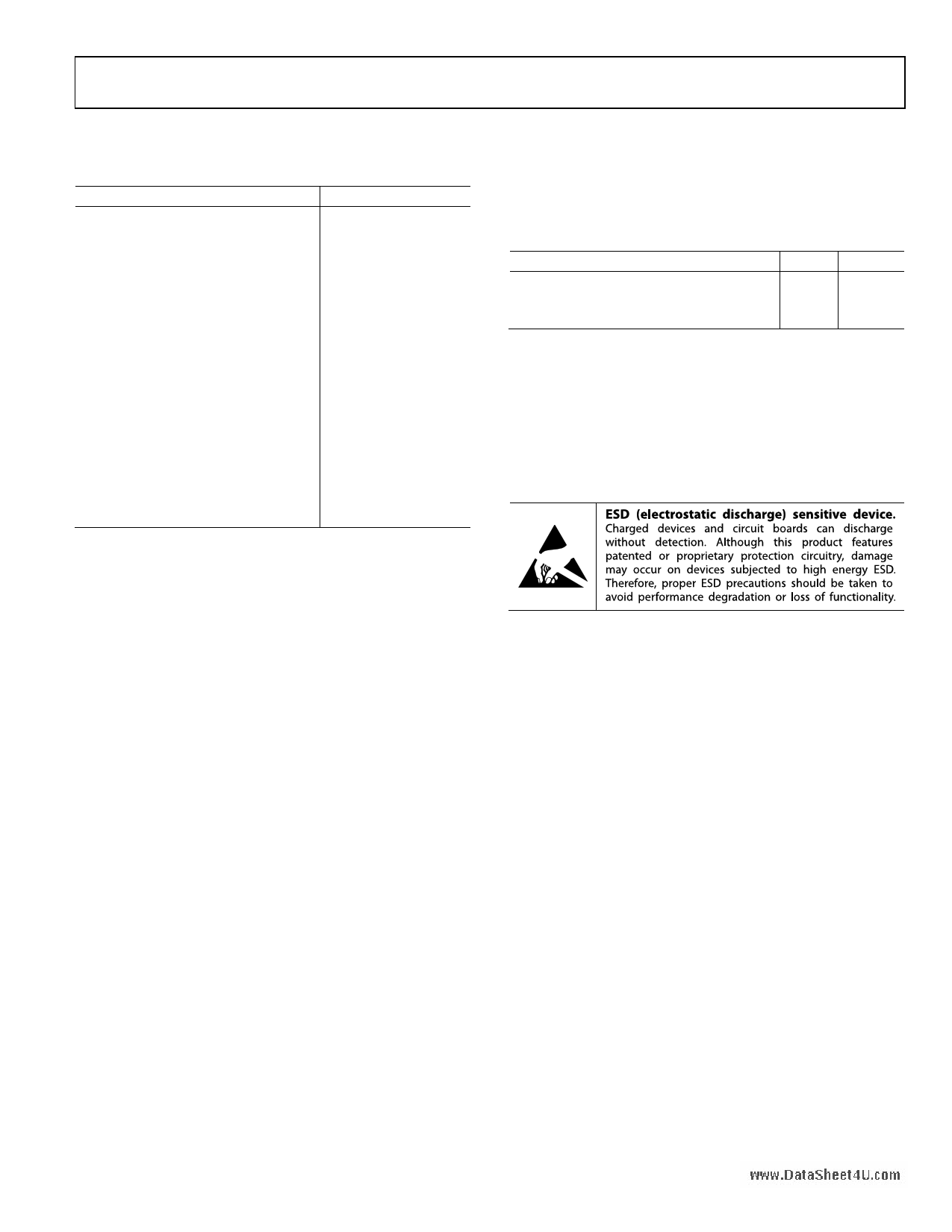
VDD to GND
VIN to PGND
FB, COMP/EN to GND
DRVL to PGND
SW to PGND
BST to SW
BST to PGND
DRVH to SW
PGND to GND
θJA (10-Lead MSOP)
2-Layer Board
4-Layer Board
Operating Junction Temperature Range
Storage Temperature Range
Soldering Conditions
Maximum Soldering Lead Temperature
(10 sec)
Rating
−0.3 V to +6 V
−0.3 V to +28 V
−0.3 V to (VDD + 0.3 V)
−0.3 V to (VDD + 0.3 V)
−2.0 V to +28 V
−0.8 V to (VDD + 0.3 V)
−0.3 V to 28 V
−0.3 V to VDD
±0.3 V
213.1°C/W
171.7°C/W
−40°C to +125°C
−65°C to +150°C
JEDEC J-STD-020
300°C
Stresses above those listed under Absolute Maximum Ratings
may cause permanent damage to the device. This is a stress
rating only; functional operation of the device at these or any
other conditions above those indicated in the operational
section of this specification is not implied. Exposure to absolute
maximum rating conditions for extended periods may affect
device reliability.
Absolute maximum ratings apply individually only, not in
combination. Unless otherwise specified, all other voltages are
referenced to PGND.
ADPw1ww8.D8a2taS/hAeeDt4UP.c1om883
THERMAL RESISTANCE
θJA is specified for the worst-case conditions, that is, a device
soldered in a circuit board for surface-mount packages.
Table 3. Thermal Resistance
Package Type
θJA (10-Lead MSOP)
2-Layer Board
4-Layer Board
θJA1 Unit
213.1 °C/W
171.7 °C/W
1 θJA is specified for the worst-case conditions; that is, θJA is specified for device
soldered in a circuit board for surface-mount packages.
BOUNDARY CONDITION
In determining the values given in Table 2 and Table 3, natural
convection was used to transfer heat to a 4-layer evaluation board.
ESD CAUTION
Rev. 0 | Page 5 of 40
5 Page 
358
354
350
346
342
338
334
330
326
322
318
314
310
306
302
298
294
290
0
VIN = 13V
+125°C
+25°C
–40°C
VIN = 16.5V
+125°C
+25°C
–40°C
0.8k 1.6k 2.4k 3.2k 4.0k 4.8k 5.6k 6.4k 7.2k 8.0k 8.8k 9.6k
LOAD CURRENT (mA)
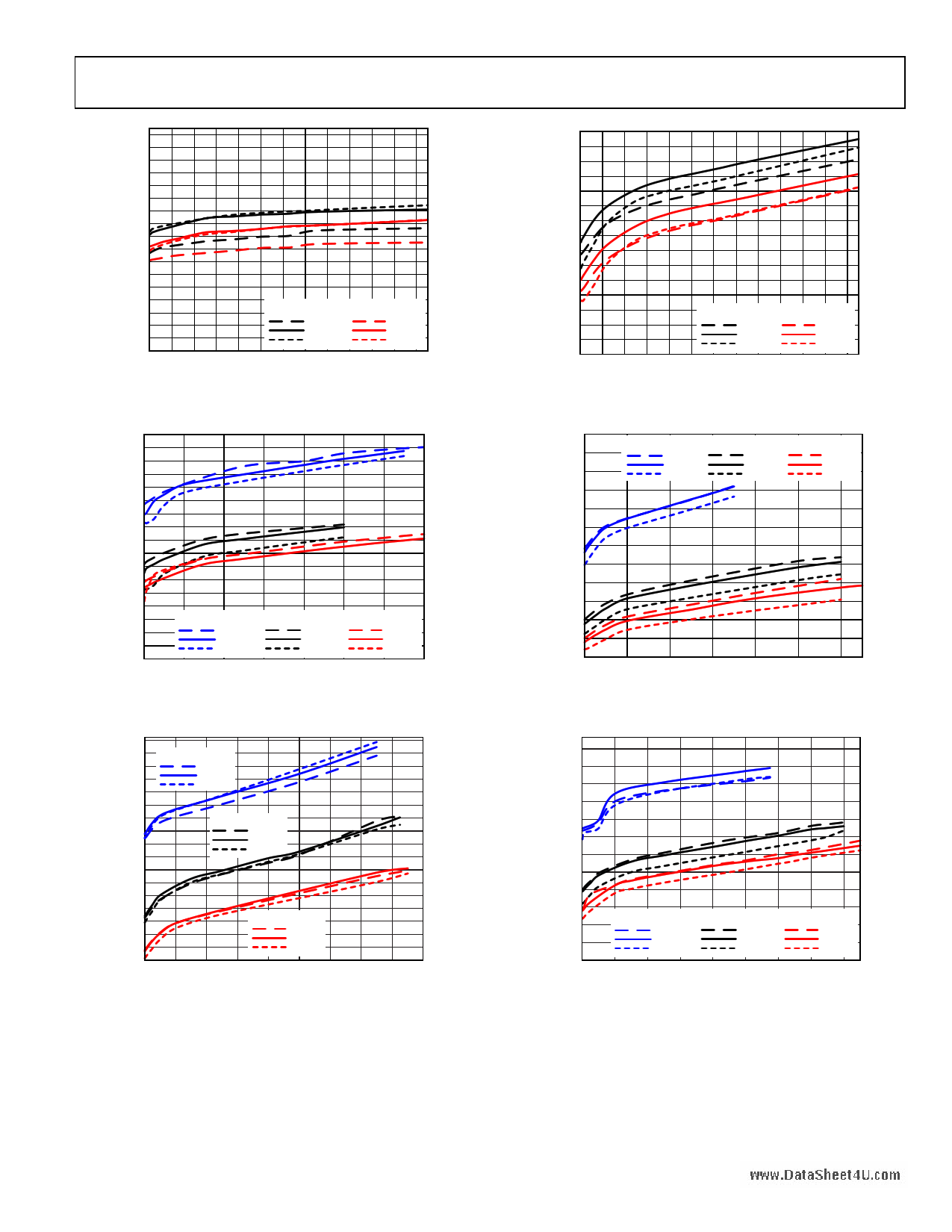
Figure 28. Frequency vs. Load Current, 300 kHz, VOUT = 7 V
700
670
640
610
580
550
520
490
460
430
400
370
340
310
280
250
220
190
0
VIN = 5.5V
+125°C
+25°C
–40°C
VIN = 13V
+125°C
+25°C
–40°C
VIN = 16.5V
+125°C
+25°C
–40°C
2k 4k 6k 8k 10k 12k 14k
LOAD CURRENT (mA)
Figure 29. Frequency vs. Load Current, 600 kHz, VOUT = 0.8 V
835
815
795
775
755
735
715
695
675
655
635
615
595
575
555
535
515
495
0
VIN = 5.5V
+125°C
+25°C
–40°C
VIN = 13V
+125°C
+25°C
–40°C
VIN = 16.5V
+125°C
+25°C
–40°C
2k 4k 6k 8k 10k 12k 14k 16k 18k
LOAD CURRENT (mA)
Figure 30. Frequency vs. Load Current, 600 kHz, VOUT = 1.8 V
ADPw1ww8.D8a2taS/hAeeDt4UP.co1m883
750
742
734
726
718
710
702
694
686
678
670
662
654
646
638
630
0
VIN = 13V
+125°C
+25°C
–40°C
VIN = 16.5V
+125°C
+25°C
–40°C
0.8k 1.6k 2.4k 3.2k 4.0k 4.8k 5.6k 6.4k 7.2k 8.0k 8.8k 9.6k
LOAD CURRENT (mA)
Figure 31. Frequency vs. Load Current, 600 kHz, VOUT =5 V
1300
1225
1150
1075
VIN = 5.5V
+125°C
+25°C
–40°C
VIN = 13V
+125°C
+25°C
–40°C
VIN = 16.5V
+125°C
+25°C
–40°C
1000
925
850
775
700
625
550
475
400
0
2k 4k 6k 8k 10k 12k
LOAD CURRENT (mA)
Figure 32. Frequency vs. Load Current, VOUT = 1.0 MHz, 0.8 V
1450
1375
1300
1225
1150
1075
1000
925
850
775
700
625
550
0
VIN = 5.5V
+125°C
+25°C
–40°C
VIN = 13V
+125°C
+25°C
–40°C
VIN = 16.5V
+125°C
+25°C
–40°C
2k 4k 6k 8k 10k 12k 14k 16k
LOAD CURRENT (mA)
Figure 33. Frequency vs. Load Current, 1.0 MHz, VOUT = 1.8 V
Rev. 0 | Page 11 of 40
11 Page | ||
| Páginas | Total 30 Páginas | |
| PDF Descargar | [ Datasheet ADP1882.PDF ] | |
Hoja de datos destacado
| Número de pieza | Descripción | Fabricantes |
| ADP1882 | Synchronous Current-Mode | Analog Devices |
| ADP1883 | Synchronous Current-Mode | Analog Devices |
| Número de pieza | Descripción | Fabricantes |
| SLA6805M | High Voltage 3 phase Motor Driver IC. |
Sanken |
| SDC1742 | 12- and 14-Bit Hybrid Synchro / Resolver-to-Digital Converters. |
Analog Devices |
|
DataSheet.es es una pagina web que funciona como un repositorio de manuales o hoja de datos de muchos de los productos más populares, |
| DataSheet.es | 2020 | Privacy Policy | Contacto | Buscar |
