|
|
|
PDF XCM519 Data sheet ( Hoja de datos )
| Número de pieza | XCM519 | |
| Descripción | 600mA Synchronous Step-Down DC/DC Converter Low Voltage Input LDO | |
| Fabricantes | Torex Semiconductor | |
| Logotipo | ||
Hay una vista previa y un enlace de descarga de XCM519 (archivo pdf) en la parte inferior de esta página. Total 30 Páginas | ||
|
No Preview Available !
XCM519 Series
www.DataSheet4U.com
ETR2421-003
600mA Synchronous Step-Down DC/DC Converter + Low Voltage Input LDO
GENERAL DESCRIPTION
The XCM519 series is a multi combination module IC which comprises of a 600mA driver transistor built-in synchronous
step–down DC/DC converter and a low voltage input LDO regulator. The device is housed in small USP-12B01 package which
is ideally suited for space conscious applications. Battery operated portable products require high efficiency so that a dual
DC/DC converter is often used. The XCM519 can replace this dual DC/DC to eliminate one inductor and reduce output noise.
The DC/DC converter and the LDO regulator blocks are isolated in the package so that noise interference from the DC/DC to
the LDO regulator is minimal.
A low output voltage and low On-resistance LDO regulator is added in series to the DC/DC output so that one another low output
voltage is created with a high efficiency and low noise. With comparison to the dual DC/DC solution, one inductor can be
eliminated which results in parts reduction and board space saving.
APPLICATIONS
Mobile phones, Smart phones
Bluetooth equipment
Portable communication modems
Portable game consoles
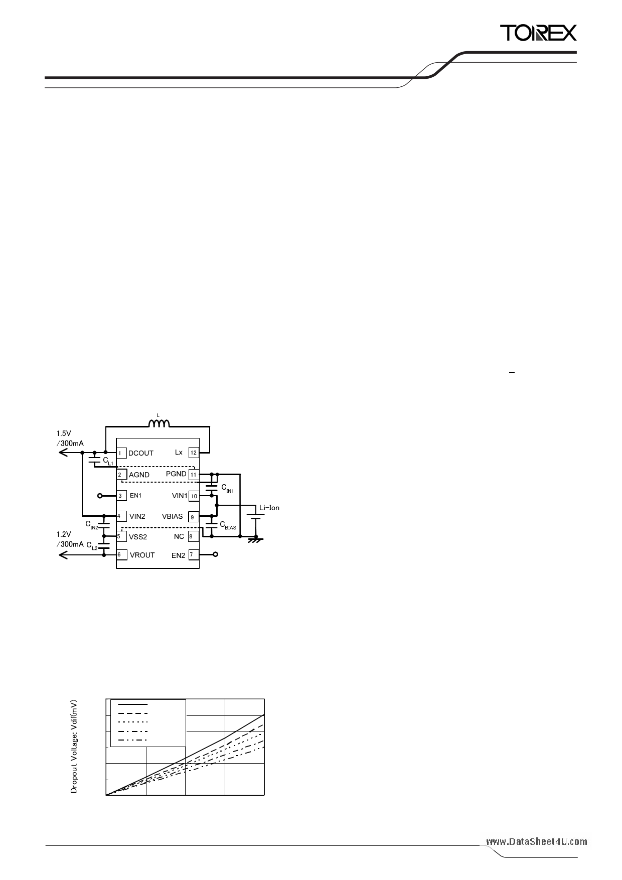
TYPICAL APPLICATION CIRCUIT
(TOP VIEW)
* The dashed lines denote the connection using
through-holes at the backside of the PC board.
TYPICAL PERFORMANCE
CHARACTERISTICS
Dropout Voltage vs. Output Current
V R O UT= 1 .2 V
300
250
200
150
VBIAS=3.0V
VBIAS=3.3V
VBIAS=3.6V
VBIAS=4.2V
VBIAS=5.0V
Ta=25℃
100
50
0
0 100 200 300 400
Output Current: IOUT(mA)
FEATURES
<DC/DC Convertor Block>
Input Voltage Range : 2.7V ~ 6.0V
Output Voltage Range : 0.8V ~ 4.0V
High Efficiency
Output Current
: 92% (TYP.)
: 600mA (MAX.)
Oscillation Frequency : 1.2MHz, 3.0MHz (+15%)
Maximum Duty Cycle : 100%
Soft-Start Circuit Built-In
Current Limiter Circuit(Constant Current & Latching)
Built-In
Control Methods
: PWM (XCM519A)
PWM/PFM Auto (XCM519B)
*Performance depends on external components and wiring on PCB wiring.
<Regulator Block>
Maximum Output Current : 400mA (Limiter 550mA TYP.)
Dropout Voltage
Bias Voltage Range
Input Voltage Range
Output Voltage Range
: 35mV@IOUT=100mA (TYP.)
(at VBIAS - VROUT(E)=2.4V)
: 2.5V ~ 6.0V (VBIAS - VROUT(E)=0.9V)
: 1.0V ~ 3.0V (VIN2 VBIAS)
: 0.7V ~ 1.8V (0.05V increments)
High Output Accuracy : ±20mV
Supply Current
Stand-by Current
UVLO
Thermal Shut Down
: IBIAS=25 A IIN2=1.0 A (TYP.)
: IBIAS=0.01 A , IIN2=0.01 A (TYP.)
: VBIAS=2.0V , VIN2=0.4V (TYP)
: Detect 150 , Release 125 (TYP.)
Soft-start Time
: 240 s VROUT=1.2V(TYP.)
CL High Speed Auto-Discharge
Low ESR Capacitor
Operating Temperature Range
Package
: Ceramic Capacitor Compatible
: -40 ~ +85
: USP-12B01
Standard Voltage Combinations : DC/DC
VR
XCM519xx01Dx
1.8V
1.2V
XCM519xx02Dx
1.8V
1.5V
XCM519xx03Dx
1.5V
1.2V
XCM519xx04Dx
1.8V
1.0V
XCM519xx05Dx
1.5V
1.0V
*Other combinations are available as semi-custom products.
1/49
1 page 
ELECTRICAL CHARACTERISTICS
XCM519xA (DC/DC BLOCK)
VDCOUT=1.8V, fOSC=1.2MHz, Ta=25
XCM519
www.DataSheet4US.coemries
PARAMETER
SYMBOL
CONDITIONS
MIN. TYP. MAX. UNITS CIRCUIT
Output Voltage
VDCOUT
When connected to external components,
VIN1 = VEN1 =5.0V, IOUT1 =30mA
1.764 1.800 1.836 V
Operating Voltage Range
VIN1
2.7 -
6.0 V
Maximum Output Current
UVLO Voltage
IOUT1MAX
VUVLO
When connected to external components,
VIN1=DCOUT(E)+2.0V, VEN1=1.0V (*8)
VEN1=VIN1, DCOUT=0V,
Voltage which Lx pin holding “L” level (*1, *10)
600 -
-
1.00 1.40 1.78
mA
V
Supply Current
IDD
VIN1=VEN1=5.0V, DCOUT=DCOUT(E)×1.1V
(XCM519AA)
(XCM519BA)
-
-
22 50
15 33
Stand-by Current
ISTB VIN1=5.0V, VEN1=0V, DCOUT=DCOUT(E)×1.1V
- 0 1.0 A
Oscillation Frequency
PFM Switching Current
PFM Duty Limit
fOSC
DLIMIT_PFM
When connected to external components,
VIN1=DCOUT(E)+2.0V,VEN1=1.0V, IOUT1=100mA (*11)
When connected to external components,
VIN1=VDCOUT(E)+2.0V, VEN1 =VIN1, IOUT1=1mA (*11)
VEN1=VIN1=(C-1), IOUT1=1mA (*11)
1020 1200 1380 kHz
120 160 200 mA
- 200 -
%
Maximum Duty Ratio
DMAX
VIN1= VEN1 =5.0V, DCOUT=DCOUT(E)×0.9V
100 -
-%
Minimum Duty Ratio
Efficiency (*2)
DMIN
EFFI
Lx SW "H" ON Resistance 1
Lx SW "H" ON Resistance 2
Lx SW "L" ON Resistance 1
Lx SW "L" ON Resistance 2
Lx SW "H" Leak Current (*5)
Lx SW "L" Leak Current (*5)
Current Limit (*9)
Output Voltage
Temperature
Characteristics
RLXH
RLXH
RLXL
RLXL
ILEAKH
ILEAKL
ILIM
DCOUT /
(DCOUT topr)
EN1 "H" Level Voltage
VEN1H
EN1 "L" Level Voltage
VEN1L
VIN1= VEN1 =5.0V, DCOUT=DCOUT(E)×1.1V
When connected to external components,
VEN1=VIN1 DCOUT(E)+1.2V (*7), IOUT1 =100mA
VIN1= VEN1 =5.0V, DCOUT=0V,ILX=100mA (*3)
VIN1= VEN1 =3.6V, DCOUT=0V,ILX=100mA (*3)
VIN1= VEN1 =5.0V (*4)
VIN1= VEN1=3.6V (*4)
VIN1= DCOUT=5.0V, VEN1 =0V, VLX=0V
VIN1= DCOUT=5.0V, VEN1 =0V, VLX=5.0V
VIN1=VEN1=5.0V, DCOUT=DCOUT(E)×0.9V
IOUT1 =30mA
-40 Topr 85
DCOUT=0V, Applied voltage to VEN,
Voltage changes Lx to “H” level (*10)
DCOUT=0V, Applied voltage to VEN,
Voltage changes Lx to “L” level (*10)
- - 0%
- 92 - %
-
0.35 0.55
Ω
-
0.42 0.67
Ω
-
0.45 0.66
Ω
-
0.52 0.77
Ω
- 0.01 1.0
A
- 0.01 1.0
A
900 1050 1350 mA
- ±100 - ppm/
0.65 -
6.0 V
VSS - 0.25 V
EN1 "H" Current
IEN1H
VIN1=VEN1=5.0V, DCOUT=0V
- 0.1
-
0.1
A
EN1 "L" Current
IEN1L
VIN1=5.0V, VEN1 =0V, DCOUT=0V
- 0.1
-
0.1
A
Soft Start Time
Latch Time
tSS
When connected to external components,
VEN1 =0V → VIN1, IOUT1=1mA
tLAT
VIN= VEN=5.0V, DCOUT=0.8× DCOUT(E)
Short Lx at 1Ω resistance (*6)
0.5 1.0 2.5 ms
1.0 - 20.0 ms
Short Protection
Threshold Voltage
VSHORT
Sweeping DCOUT, VIN1=VEN1= 5.0V, Short Lx at
1Ω resistance, DCOUT voltage which Lx becomes
“L” level within 1ms
0.675 0.900 1.125
V
Test conditions: Unless otherwise stated, VIN = 5.0V, VDCOUT(E)= Setting voltage
NOTE:
*1: Including hysteresis width of operating voltage.
*2: EFFI = { ( output voltage output current ) ( input voltage input current) } 100
*3: ON resistance ( )= (VIN - Lx pin measurement voltage) 100mA
*4: Design value
*5: When temperature is high, a current of approximately 10 A (maximum) may leak.
*6: Time until it short-circuits DCOUT with GND via 1 of resistor from an operational state and is set to Lx=0V from current limit pulse
generating.
*7: VDCOUT (E)+1.2V<2.7V, VIN=2.7V.
*8: When the difference between the input and the output is small, some cycles may be skipped completely before current maximizes.
If current is further pulled from this state, output voltage will decrease because of P-ch driver ON resistance.
*9: Current limit denotes the level of detection at peak of coil current.
*10: "H" VIN VIN - 1.2V, "L" + 0.1V - 0.1V
*11: XCM519A series exclude IPFM and MAXIPFM because those are only for the PFM control’s functions.
* The electrical characteristics above are when the other channel is in stop mode.
5/49
5 Page 
XCM519
www.DataSheet4US.coemries
ELECTRICAL CHARACTERISTICS (Continued)
XCM519xx 2ch (REGULATOR BLOCK) (Continued)
PARAMETER
SYMBOL
CONDITIONS
Output Voltage
Temperature
Characteristics
Limit Current
Short Current
Thermal Shutdown
Detect Temperature
VROUT/ VBIAS=VEN2=3.6V, VIN2=VROUT(T)+0.3V , IOUT=30mA,
( Topr VROUT)
- 40 Topr 85
ILIM
ISHORT
VROUT=VROUT(T) 0.95,
VBIAS=VEN2=3.6V, VIN2=VROUT(T)+0.3V
VBIAS=VEN2=3.6V, VIN2=VROUT(T)+0.3V,
VROUT=0V
TTSD
Junction Temperature
Thermal Shutdown
Release Temperature
TTSR
Junction Temperature
TSD Hysteresis Width TTSD TTSR
CL Auto-Discharge
Resistance
EN2 "H" Level Voltage
EN2 "L" Level Voltage
EN2 "H" Level Current
EN2 "L" Level Current
Soft Start Time (*11)
RDCHG
VEN2H
VEN2L
IEN2H
IEN2L
tSS
VBIAS=3.6V, VIN2= VROUT(T)+0.3V, VEN2= VSS
VROUT=VROUT(T)
VBIAS=3.6V,VIN2=VROUT(T)+0.3V
VBIAS=3.6V,VIN2=VROUT(T)+0.3V
VBIAS=VEN2=6.0V,
VIN2=VROUT(T)+0.3V
VBIAS=6.0V, VEN2=VSS,VIN2=VROUT(T)+0.3V
VBIAS=3.6V VIN2=VROUT(T)+0.3V IOUT=1mA
VEN2=0V 3.6V
MIN.
-
400
-
-
-
-
290
0.75
-
-0.1
-0.1
100
TYP.
100
-
80
150
125
25
430
-
-
-
-
-
MAX. UNITS CIRCUIT
- ppm/
- mA
- mA
-
-
-
610
6.0
0.16
0.1
0.1
410
V
V
A
A
s
NOTE:
* 1: Please use Bias voltage VBIAS within the range VBIAS –VROUT(T) 0.9V
* 2: Please use Input voltage VIN within the range VIN VBIAS
* 3: VROUT(E) : Effective output voltage
* 4: VROUT(T) : Specified output voltage
* 5: E-0 = Please refer to the table named OUTPUT VOLTAGE CHART
* 6: E-1 = Please refer to the table named DROPOUT VOLTAGE CHART
* 7: Vdif={VIN21(*8) -VROUT1(*9)}
* 8: VIN21 : The input voltage when VOUT1 appears as input voltage is gradually decreased.
* 9: VROUT1 : A voltage equal to 98% of the output voltage while maintaining an amply stabilized output voltage when VBIAS<3.0V at VIN2= VBIAS,
VBIAS 3.0V at VIN2=VBIAS input to the VBIAS pin.
*10 : IBIASMAX : A supply current at the VBIAS pin providing for the output current (IVROUT) .
*11: tSS : Time that VROUT becomes more than VROUT(E) 0.9V after the EN2 pin is input 0.75V as EN2 “H” level voltage.
* The electrical characteristics above are when the other channel is in stop mode.
OUTPUT VOLTAGE CHART
NOMINAL OUTPUT
VOLTAGE (V)
E-0
OUTPUT VOLTAGE (V)
VROUT
VROUT(T)
MIN.
MAX.
0.70
0.680
0.720
0.75
0.730
0.770
0.80
0.780
0.820
0.85
0.830
0.870
0.90
0.880
0.920
0.95
0.930
0.970
1.00
0.980
1.020
1.05
1.030
1.070
1.10
1.080
1.120
1.15
1.130
1.170
1.20
1.180
1.220
1.25
1.230
1.270
NOMINAL OUTPUT
VOLTAGE (V)
VROUT(T)
1.30
1.35
1.40
1.45
1.50
1.55
1.60
1.65
1.70
1.75
1.80
E-0
OUTPUT VOLTAGE (V)
MIN.
VROUT
MAX.
1.280
1.320
1.330
1.370
1.380
1.420
1.430
1.470
1.480
1.520
1.530
1.570
1.580
1.620
1.630
1.670
1.680
1.720
1.730
1.770
1.780
1.820
11/49
11 Page | ||
| Páginas | Total 30 Páginas | |
| PDF Descargar | [ Datasheet XCM519.PDF ] | |
Hoja de datos destacado
| Número de pieza | Descripción | Fabricantes |
| XCM517 | 600mA Synchronous Dual Output Step-Down DC/DC Converters | Torex Semiconductor |
| XCM519 | 600mA Synchronous Step-Down DC/DC Converter Low Voltage Input LDO | Torex Semiconductor |
| Número de pieza | Descripción | Fabricantes |
| SLA6805M | High Voltage 3 phase Motor Driver IC. |
Sanken |
| SDC1742 | 12- and 14-Bit Hybrid Synchro / Resolver-to-Digital Converters. |
Analog Devices |
|
DataSheet.es es una pagina web que funciona como un repositorio de manuales o hoja de datos de muchos de los productos más populares, |
| DataSheet.es | 2020 | Privacy Policy | Contacto | Buscar |