|
|
|
PDF A8735 Data sheet ( Hoja de datos )
| Número de pieza | A8735 | |
| Descripción | Ultra Small Mobile Phone Xenon Photoflash Capacitor Charger | |
| Fabricantes | Allegro Micro Systems | |
| Logotipo | ||
Hay una vista previa y un enlace de descarga de A8735 (archivo pdf) en la parte inferior de esta página. Total 16 Páginas | ||
|
No Preview Available !
A8735www.DataSheet4U.com
Ultra Small Mobile Phone Xenon Photoflash
Capacitor Charger with IGBT Driver
Features and Benefits
▪ Ultra small 2 × 2 DFN/MLP-8 package
▪ Low quiescent current draw (0.5 μA max. in shutdown mode)
▪ Primary-side output voltage sensing; no resistor divider required
▪ Fixed 1 A peak current limit
▪ 1V logic (VHI(min)) compatibility
▪ Integrated IGBT driver with internal gate resistors
▪ Optimized for mobile phone, 1-cell Li+ battery applications
▪ Zero-voltage switching for lower loss
▪ >75% efficiency
▪ Charge complete indication
▪ Integrated 50 V DMOS switch with self-clamping protection
Package: 8-pin DFN/MLP (suffix EE)
Description
TheAllegro®A8735 is a Xenon photoflash charger IC designed
to meet the needs of ultra low power, small form factor cameras,
particularly camera phones. By using primary-side voltage
sensing, the need for a secondary-side resistive voltage divider
is eliminated.This has the additional benefit of reducing leakage
currents on the secondary side of the transformer. To extend
battery life, the A8735 features very low supply current draw
(0.5 μA max in shutdown mode). The IGBT driver also has
internal gate resistors for minimum external component count.
The charge and trigger voltage logic thresholds are set at 1
VHI(min) to support applications implementing low-voltage
control logic.
The A8735 is available in an 8-contact 2 mm × 2 mm
DFN/MLP package with a 0.60 maximum overall package
height, and an exposed pad for enhanced thermal performance.
It is lead (Pb) free with 100% matte tin leadframe plating.
Not to scale
2 mm × 2 mm, 0.60 mm height
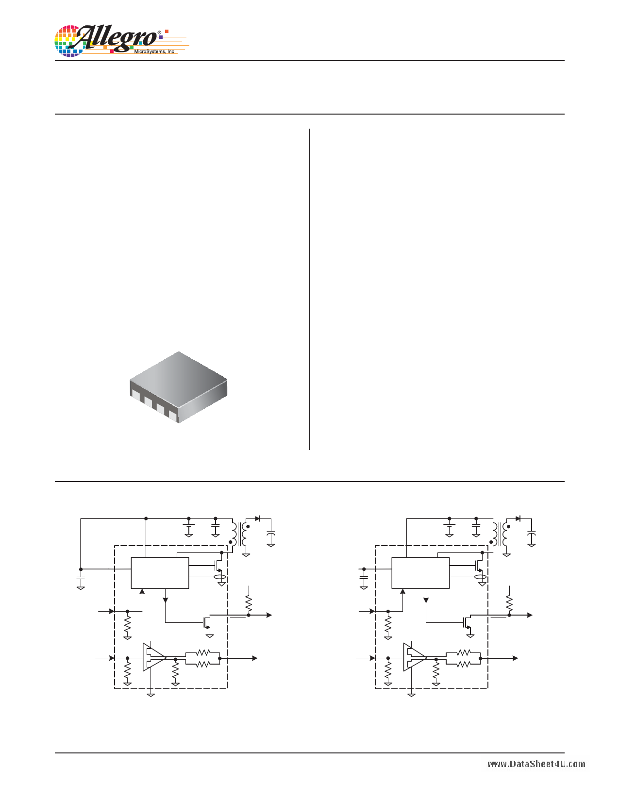
Typical Applications
VIN_VDRV
C2
CHARGE
TRIG
Battery Input +
2.3 to 5.5 V
C1
VBAT
VOUT Detect
SW
Control
Block
ISW sense
COUT
100F
315 V
VPULLUP
DONE
100 kΩ
DONE
VIN_VDRV
IGBT Driver
IGBT Gate
GATE
VIN_VDRV
C2
CHARGE
TRIG
Battery Input +
1.5 to 5.5 V
C1
VBAT
VOUT Detect
SW
Control
Block
ISW sense
COUT
100F
315 V
VPULLUP
DONE
100 kΩ
DONE
VIN_VDRV
IGBT Driver
IGBT Gate
GATE
GND
(A)
GND
(B)
Figure 1. Typical applications: (A) with single battery supply and (B) with separate bias supply
8735-DS
1 page 
A8735
Ultra Small Mobile Phone Xenon Photoflashwww.DataSheet4U.com
Capacitor Charger with IGBT Driver
IGBT Drive Timing Definition
TRIG
GATE
50%
50%
tDr tr
tDf tf
10%
90%
90%
10%
Operation Timing Diagram
VBAT
VIN UVLO
CHARGE
SW
Target VOUT
VOUT
DONE
TRIG
T1
T2
T3
GATE
A
B
C
DE
F
Explanation of Events
A: Start charging by pulling CHARGE to high, provided that VIN is above UVLO level.
B: Charging stops when VOUT reaches the target voltage.
C: Start a new charging process with a low-to-high transition at the CHARGE pin.
D: Pull CHARGE to low to put the controller in low-power standby mode.
E: Charging does not start, because VIN is below UVLO level when CHARGE goes high.
F: After VIN goes above UVLO, another low-to-high transition at the CHARGE pin is required to
start the charging.
T1, T2, T3 (Trigger instances): IGBT driver output pulled high whenever the TRIG pin is at logic
high. It is recommended to avoid applying any trigger pulses during charging.
Allegro MicroSystems, Inc.
115 Northeast Cutoff
Worcester, Massachusetts 01615-0036 U.S.A.
1.508.853.5000; www.allegromicro.com
5
5 Page 
A8735
Ultra Small Mobile Phone Xenon Photoflashwww.DataSheet4U.com
Capacitor Charger with IGBT Driver
As soon as a sufficient voltage has built up at the output capaci-
tor, the IC enters Fast-Charging mode. In this mode, the next
switching cycle starts after the secondary side current has stopped
flowing, and the switch voltage has dropped to a minimum value.
A proprietary circuit is used to allow minimum-voltage switch-
ing, even if the SW pin voltage does not drop to 0 V. This enables
Fast-Charging mode to start earlier, thereby reducing the overall
charging time. Minimum-voltage switching is shown in figure 4.
During Fast-Charging mode, when VOUT is high enough (over
50 V), true zero-voltage switching (ZVS) is achieved. This
further improves efficiency as well as reduces switching noise. A
ZVS interval is shown in figure 5.
C4
ISW
C4
ISW
C2,C3
VSW
VBAT
VOUT
C1
Figure 4. Minimum-voltage switching: VOUT ≥ 35 V, VBAT = 5.5 V,
Ch1: VOUT = 20 V / div., Ch2: VBAT = 5 V / div., Ch3: VSW = 5 V / div.,
Ch4: ISW = 500 mA/ div., t = 1 μs / div.
C2,C3
VSW
VBAT
VOUT
C1
Figure 5. True zero-voltage switching (ZVS): VOUT = 75 V, VBAT = 5.5 V,
Ch1: VOUT = 20 V / div., Ch2: VBAT = 5 V / div., Ch3: VSW = 5 V / div.,
Ch4: ISW = 500 mA/ div., t = 0.5 μs / div.
Allegro MicroSystems, Inc.
115 Northeast Cutoff
Worcester, Massachusetts 01615-0036 U.S.A.
1.508.853.5000; www.allegromicro.com
11
11 Page | ||
| Páginas | Total 16 Páginas | |
| PDF Descargar | [ Datasheet A8735.PDF ] | |
Hoja de datos destacado
| Número de pieza | Descripción | Fabricantes |
| A8732 | Ultra Small Mobile Phone Xenon Photoflash Capacitor Charger | Allegro Micro Systems |
| A8735 | Ultra Small Mobile Phone Xenon Photoflash Capacitor Charger | Allegro Micro Systems |
| Número de pieza | Descripción | Fabricantes |
| SLA6805M | High Voltage 3 phase Motor Driver IC. |
Sanken |
| SDC1742 | 12- and 14-Bit Hybrid Synchro / Resolver-to-Digital Converters. |
Analog Devices |
|
DataSheet.es es una pagina web que funciona como un repositorio de manuales o hoja de datos de muchos de los productos más populares, |
| DataSheet.es | 2020 | Privacy Policy | Contacto | Buscar |