|
|
|
PDF RF5755 Data sheet ( Hoja de datos )
| Número de pieza | RF5755 | |
| Descripción | 2.4GHz 802.11b/g/n WLAN FRONT-END MODULE | |
| Fabricantes | RF Micro Devices | |
| Logotipo | ||
Hay una vista previa y un enlace de descarga de RF5755 (archivo pdf) en la parte inferior de esta página. Total 12 Páginas | ||
|
No Preview Available !
RF5755www.DataSheet4U.com
3.3V, 2.4GHz 802.11b/g/n WLAN
FRONT-END MODULE
Package Style: QFN, 16-pin, 3mmx3mmx0.5mm
Features
Integrated 2.5GHz b/g/n
Amplifier, LNA, SP3T Switch,
and Power Detector Coupler
Single Supply Voltage 3.0V to
4.8 V
POUT=20dBm, 11g, OFDM at
<4% EVM, 23dBm 11b
Meeting 11b Spectral Mask
Applications
IEEE802.11b/g/n WLAN
2.5GHz ISM Band Solutions
Portable Battery-Powered
Equipment
16 15 14 13
LNA VDD 1
12 C_BT
RX OUT 2
VREG 3
11 ANT
SP3T
10 GND
TX IN 4
9 N/C
5678
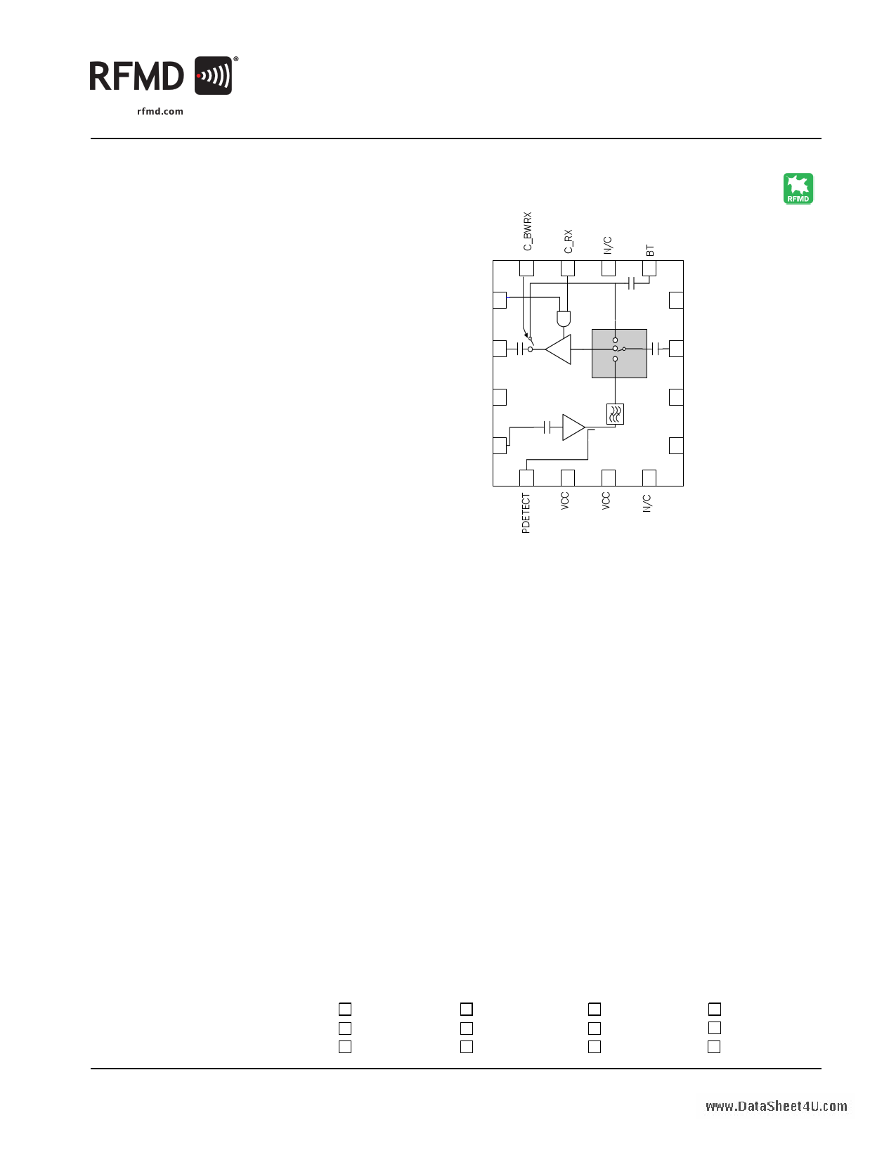
Functional Block Diagram
Product Description
The RF5755 provides a complete integrated solution in a single Front End
Module (FEM) for WLAN 802.11b/g/n and Bluetooth® systems. The ultra
small form factor and integrated matching greatly reduces the number of
external components and layout area in the customer application. This
simplifies the total Front End solution by reducing the bill of materials, sys-
tem footprint, and manufacturability cost. The RF5755 integrates a
2.4GHz Power Amplifier (PA), Low Noise Amplifier (LNA), power detector
coupler for improved accuracy, and some filtering for harmonic rejection.
The RF5755 is capable of receiving WLAN and Bluetooth® simultaneously.
The device is provided in a 3mmx3mmx0.5mm, 16-pin package. This
module meets or exceeds the RF Front End needs of IEEE 802.11b/g/n
WLAN RF systems.
Ordering Information
RF5755
RF5755PCK-410
3.3V, 2.4GHz 802.11b/g/n WLAN Front-End Module
Fully Assembled Evaluation Board with 5pcs Sample
DS100324
Optimum Technology Matching® Applied
9GaAs HBT
SiGe BiCMOS
9GaAs pHEMT
GaN HEMT
GaAs MESFET
Si BiCMOS
Si CMOS
RF MEMS
InGaP HBT
SiGe HBT
Si BJT
LDMOS
RF MICRO DEVICES®, RFMD®, Optimum Technology Matching®, Enabling Wireless Connectivity™, PowerStar®, POLARIS™ TOTAL RADIO™ and UltimateBlue™ are trademarks of RFMD, LLC. BLUETOOTH is a trade-
mark owned by Bluetooth SIG, Inc., U.S.A. and licensed for use by RFMD. All other trade names, trademarks and registered trademarks are the property of their respective owners. ©2006, RF Micro Devices, Inc.
7628 Thorndike Road, Greensboro, NC 27409-9421 · For sales or technical
support, contact RFMD at (+1) 336-678-5570 or [email protected].
1 of 12
1 page 
RF5755www.DataSheet4U.com
Parameter
Specification
Min. Typ. Max.
Unit
Condition
Other Requirements, cont.
ESD
Human Body Model 500
V EIA/JESD22-114A RF pins
1000
V EIA/JESD22-114A DC pins
Charge Device Model 500
V JESD22-C101C all pins
Note 1: The PA module must operate with gated bias voltage input at 1% to 99% duty cycle.
Note 3: Values to be agreed to upon characterization data review: current, gain, return loss, detector sensitivity and output power.
Note 4: The output power for channels 1 and 11 may be reduced to meet FCC restricted band requirements.
Switch Control Logic
Mode
VREG
C RX
C BT C BWRx
Standby
LLLL
WLAN TX
HL L L
WLAN RX
LHL L
WLAN RX/BT*
LHLH
BT RX
L LHL
BT TX
L LHL
*The FEM can be placed in receive WLAN and Bluetooth® modes simultaneously with increased insertion loss.
DS100324
7628 Thorndike Road, Greensboro, NC 27409-9421 · For sales or technical
support, contact RFMD at (+1) 336-678-5570 or [email protected].
5 of 12
5 Page 
RF5755www.DataSheet4U.com
The RF755 WLAN and Bluetooth® receive circuits were specifically designed to address issues of simultaneous operation. In
this mode both signals can be received at the same time when the C_BWRX (pin-16) is set high. The typical gain for each RF
path is approximately 13dB and a NF of 3dB. During simultaneous mode the active components are the LNA, the SPST switch,
and only the RX branch of the SP3T. Refer to the logic control table for proper settings.
Simultaneous Mode Biasing Instructions
• Connect the RF input (ANT/pin-11) to a signal generator and a spectrum analyzer at the RX (pin-2) and BT (pin-13) RF ports.
A multiport VNA may be used as well.
• Turn the LNA bias ON (pin-1) and set the voltage to 3.3V
• Set C_RX (pin-15) and C_BWRX (pin-16) high. This turns ON the receive branch of the SP3T and the SPST switch.
• The SP3T controls for the off branches (VREG and C_BT) must be set to a logic “low” (0.2V max) or grounded. In the event
that one of these branches is left floating or in a logic “high” the performance will degrade. It is recommended to terminate
unused RF Ports in 50Ω.
• Turn RF ON
BLUETOOTH® MODE
The RF755 Bluetooth® only mode is implemented through the SP3T switch by setting C_BT “high.” Typical insertion loss is
about 1.2dB.
Bluetooth® Biasing Instructions
• Connect the RF input (ANT/pin-11) to a signal generator and a spectrum analyzer at the BT (pin-13) RF port. A VNA may be
used in place of the Sig Gen and SA.
• Set C_BT (pin-12) “high.” This turns the Bluetooth® branch of the SP3T switch ON.
• The SP3T controls for the off branches (VREG and C_RX) must be set to a logic “low” (0.2V max) or grounded. Do not leave
floating.
• Terminate unused RF Ports in 50Ω
• Turn RF ON
APPLICATION CIRCUIT AND LAYOUT RECOMMENDATIONS
The RF5755 integrates the matching networks and DC blocking capacitors for all RF ports. This greatly reduces the number of
external components and layout area needed to implement this FEM. Typically only a total of four external components are
required to achieve nominal performance. However, depending on board layout and the many noise signals that could poten-
tially couple to the RF5755, additional bypassing capacitors may be required to properly filter out unwanted signals that might
degrade performance.
The LNA bias components consist of an inductor and a decoupling capacitor. The inductor value is critical to optimize NF and
return loss at the RX output. For best performance and trade off between critical parameters such as NF, Gain, and IP3, the
total inductance including board trace should be approximately 1.2nH. The 5.6kΩ series resistor for the Bluetooth® control
line helps to prevent unwanted signal from coupling to this pin. The resistor should be place as close as possible to the pack-
age pin. The last component needed in the application circuit is a low frequency bypass capacitor on the VCC line. In general, it
is good RF practice to have proper decoupling of supply lines to filter out noise. Occasionally, depending on the level of cou-
pling or parasitics of the board, a high frequency bypass capacitor must be added as well.
DS100324
7628 Thorndike Road, Greensboro, NC 27409-9421 · For sales or technical
support, contact RFMD at (+1) 336-678-5570 or [email protected].
11 of 12
11 Page | ||
| Páginas | Total 12 Páginas | |
| PDF Descargar | [ Datasheet RF5755.PDF ] | |
Hoja de datos destacado
| Número de pieza | Descripción | Fabricantes |
| RF5755 | 2.4GHz 802.11b/g/n WLAN FRONT-END MODULE | RF Micro Devices |
| Número de pieza | Descripción | Fabricantes |
| SLA6805M | High Voltage 3 phase Motor Driver IC. |
Sanken |
| SDC1742 | 12- and 14-Bit Hybrid Synchro / Resolver-to-Digital Converters. |
Analog Devices |
|
DataSheet.es es una pagina web que funciona como un repositorio de manuales o hoja de datos de muchos de los productos más populares, |
| DataSheet.es | 2020 | Privacy Policy | Contacto | Buscar |