|
|
|
PDF VNQ830P-E Data sheet ( Hoja de datos )
| Número de pieza | VNQ830P-E | |
| Descripción | QUAD CHANNEL HIGH SIDE DRIVER | |
| Fabricantes | ST Microelectronics | |
| Logotipo | ||
Hay una vista previa y un enlace de descarga de VNQ830P-E (archivo pdf) en la parte inferior de esta página. Total 21 Páginas | ||
|
No Preview Available !
www.DataSheet4U.com
VNQ830P-E
QUAD CHANNEL HIGH SIDE DRIVER
Table 1. General Features
TYPE
RDS(on)
IOUT
VNQ830P-E 65 mΩ (*) 6 A (*)
VCC
36 V
(*) Per each channel
s CMOS COMPATIBLE INPUTS
s OPEN DRAIN STATUS OUTPUTS
s ON STATE OPEN LOAD DETECTION
s OFF STATE OPEN LOAD DETECTION
s SHORTED LOAD PROTECTION
s UNDERVOLTAGE AND OVERVOLTAGE
SHUTDOWN
s PROTECTION AGAINST LOSS OF GROUND
s VERY LOW STAND-BY CURRENT
s REVERSE BATTERY PROTECTION (**)
s IN COMPLIANCE WITH THE 2002/95/EC
EUROPEAN DIRECTIVE
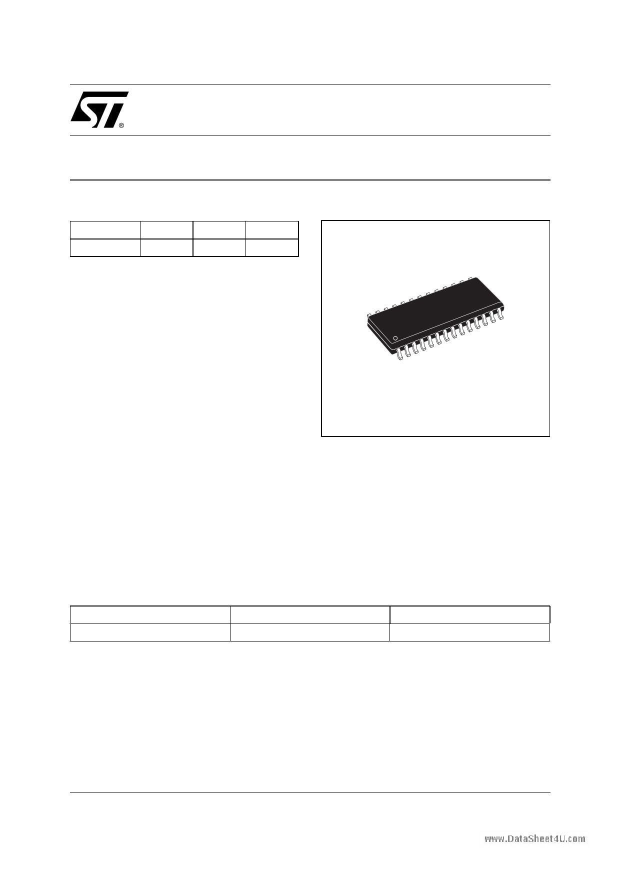
Figure 1. Package
TARGET SPECIFICATION
SO-28 (DOUBLE ISLAND)
DESCRIPTION
The VNQ830P-E is a quad HSD formed by
assembling two VND830-E chips in the same SO-
28 package. The VND830-E is a monolithic device
made by using| STMicroelectronics VIPower M0-3
Technology. The VNQ830P-E is intended for
driving any type of multiple loads with one side
connected to ground.
Active VCC pin voltage clamp protects the device
against low energy spikes (see ISO7637 transient
compatibility table).
Active current limitation combined with thermal
shutdown and automatic restart protects the
device against overload.
The device detects open load condition both in on
and off state. Output shorted to VCC is detected in
the off state. Device automatically turns off in case
of ground pin disconnection.
Table 2. Order Codes
Package
SO-28
Tube
VNQ830P-E
Tape and Reel
VNQ830PTR-E
Note: (**) See application schematic at page 11.
October 2004
Rev. 1
1/21
This is preliminary information on a new product foreseen to be developed. Details are subject to change without notice.
1 page 
VwNwQw8.D3a0tPaS-hEeet4U.com
ELECTRICAL CHARACTERISTICS (8V<VCC<36V; -40°C<Tj<150°C unless otherwise specified)
Table 5. Power Outputs (Per each channel)
Symbol
Parameter
Test Conditions
Min. Typ. Max. Unit
VCC (**) Operating Supply Voltage
5.5 13
36 V
VUSD (**) Undervoltage Shut-down
3 4 5.5 V
VOV (**) Overvoltage Shut-down
36 V
Ron On State Resistance
IOUT=2A; Tj=25°C
IOUT=2A; VCC>8V
65 mΩ
130 mΩ
IS (**) Supply Current
Off State; VCC=13V; VIN=VOUT=0V
Off State; VCC=13V; VIN=VOUT=0V;
Tj =25°C
On State; VCC=13V; VIN=5V; IOUT=0A
12 40 µA
12 25 µA
5 7 mA
IL(off1)
IL(off2)
IL(off3)
IL(off4)
Off State Output Current
Off State Output Current
Off State Output Current
Off State Output Current
VIN=VOUT=0V
VIN=0V; VOUT=3.5V
VIN=VOUT=0V; VCC=13V; Tj =125°C
VIN=VOUT=0V; VCC=13V; Tj =25°C
0
-75
50 µA
0 µA
5 µA
3 µA
Note: (**) Per island.
Table 6. Switching (Per each channel) (VCC =13V)
Symbol
Parameter
Test Conditions
td(on) Turn-on Delay Time
td(off) Turn-off Delay Time
RL=6.5Ω from VIN rising edge to
VOUT=1.3V
RL=6.5Ω from VIN falling edge to
VOUT=11.7V
dVOUT/
dt(on)
Turn-on Voltage Slope
RL=6.5Ω from VOUT=1.3V to
VOUT=10.4V
dVOUT/
dt(off)
Turn-off Voltage Slope
RL=6.5Ω from VOUT=11.7V to
VOUT=1.3V
Min.
Typ.
30
Max. Unit
µs
30
See
relative
diagram
See
relative
diagram
µs
V/µs
V/µs
Table 7. VCC - Output Diode
Symbol
Parameter
VF Forward on Voltage
Test Conditions
-IOUT=1.2A; Tj=150°C
Min Typ Max Unit
0.6 V
5/21
5 Page 
VwNwQw8.D3a0tPaS-hEeet4U.com
Solution 2: A diode (DGND) in the ground line.
A resistor (RGND=1kΩ) should be inserted in parallel to
DGND if the device will be driving an inductive load.
This small signal diode can be safely shared amongst
several different HSD. Also in this case, the presence of
the ground network will produce a shift (j600mV) in the
input threshold and the status output values if the
microprocessor ground is not common with the device
ground. This shift will not vary if more than one HSD
shares the same diode/resistor network.
Series resistor in INPUT and STATUS lines are also
required to prevent that, during battery voltage transient,
the current exceeds the Absolute Maximum Rating.
Safest configuration for unused INPUT and STATUS pin
is to leave them unconnected.
LOAD DUMP PROTECTION
Dld is necessary (Voltage Transient Suppressor) if the
load dump peak voltage exceeds VCC max DC rating.
The same applies if the device will be subject to
transients on the VCC line that are greater than the ones
shown in the ISO T/R 7637/1 table.
µC I/Os PROTECTION:
If a ground protection network is used and negative
transients are present on the VCC line, the control pins will
be pulled negative. ST suggests to insert a resistor (Rprot)
in line to prevent the µC I/Os pins to latch-up.
The value of these resistors is a compromise between the
leakage current of µC and the current required by the
HSD I/Os (Input levels compatibility) with the latch-up
limit of µC I/Os.
-VCCpeak/Ilatchup ≤ Rprot ≤ (VOHµC-VIH-VGND) / IIHmax
Calculation example:
For VCCpeak= - 100V and Ilatchup ≥ 20mA; VOHµC ≥ 4.5V
5kΩ ≤ Rprot ≤ 65kΩ.
Recommended Rprot value is 10kΩ.
OPEN LOAD DETECTION IN OFF STATE
Off state open load detection requires an external pull-up
resistor (RPU) connected between OUTPUT pin and a
positive supply voltage (VPU) like the +5V line used to
supply the microprocessor.
The external resistor has to be selected according to the
following requirements:
1) no false open load indication when load is connected:
in this case we have to avoid VOUT to be higher than
VOlmin; this results in the following condition
VOUT=(VPU/(RL+RPU))RL<VOlmin.
2) no misdetection when load is disconnected: in this
case the VOUT has to be higher than VOLmax; this
results in the following condition RPU<(VPU–VOLmax)/
IL(off2).
Because Is(OFF) may significantly increase if Vout is
pulled high (up to several mA), the pull-up resistor RPU
should be connected to a supply that is switched OFF
when the module is in standby.
The values of VOLmin, VOLmax and IL(off2) are available in
the Electrical Characteristics section.
Figure 9. Open Load detection in off state
V batt.
VPU
INPUT
STATUS
VCC
DRIVER
+
LOGIC
+
R
-
VOL
IL(off2)
OUT
RPU
RL
GROUND
11/21
11 Page | ||
| Páginas | Total 21 Páginas | |
| PDF Descargar | [ Datasheet VNQ830P-E.PDF ] | |
Hoja de datos destacado
| Número de pieza | Descripción | Fabricantes |
| VNQ830P-E | QUAD CHANNEL HIGH SIDE DRIVER | ST Microelectronics |
| Número de pieza | Descripción | Fabricantes |
| SLA6805M | High Voltage 3 phase Motor Driver IC. |
Sanken |
| SDC1742 | 12- and 14-Bit Hybrid Synchro / Resolver-to-Digital Converters. |
Analog Devices |
|
DataSheet.es es una pagina web que funciona como un repositorio de manuales o hoja de datos de muchos de los productos más populares, |
| DataSheet.es | 2020 | Privacy Policy | Contacto | Buscar |