|
|
|
PDF ICS87158 Data sheet ( Hoja de datos )
| Número de pieza | ICS87158 | |
| Descripción | LVPECL-TO-HCSL/LVCMOS | |
| Fabricantes | Integrated Circuit Systems | |
| Logotipo | ||
Hay una vista previa y un enlace de descarga de ICS87158 (archivo pdf) en la parte inferior de esta página. Total 16 Páginas | ||
|
No Preview Available !
Integrated
Circuit
Systems, Inc.
ICS87158
1-TO-6, LVPECL-TO-HCSLw/wLwV.DCatMaShOeeSt4U.com
÷1, ÷2, ÷4 CLOCK GENERATOR
GENERAL DESCRIPTION
The ICS87158 is a high performance 1-to-6
ICS LVPECL-to-HCSL/LVCMOS Clock Generator
HiPerClockS™ and is a member of the HiPerClockS™ family of
High Performance Clock Solutions from ICS. The
ICS87158 has one differential input (which can
accept LVDS, LVPECL, LVHSTL, SSTL, HCSL), six differential
HCSL output pairs and two complementary LVCMOS/LVTTL
outputs. The six HCSL output pairs can be individually con-
figured for divide-by-1, 2, and 4 or high impedance by use of
select pins. The two complementary LVCMOS/LVTTL outputs
can be configured for divide by 2, divide by 4, high imped-
ance, or driven low for low power operation.
The primary use of the ICS87158 is in Intel® E8870 chipsets
that use Intel® Pentium 4 processors. The ICS87158 converts
the differential clock from the main system clock into HCSL
clocks used by Intel® Pentium 4 processors. However, the
ICS87158 is a highly flexible, general purpose device that
operates up to 600MHz and can be used in any situation where
Differential-to-HCSL translation is required.
FEATURES
• Six HCSL outputs
• Two LVCMOS/LVTTL outputs
• One Differential LVPECL clock input pair
• PCLK, nPCLK supports the following input types:
LVDS, LVPECL, LVHSTL, SSTL, HCSL
• Maximum output frequency: 600MHz (maximum)
• Output skew: 100ps (maximum)
• Propagation delay: 4ns (maximum)
• 3.3V operating supply
• 0°C to 85°C ambient operating temperature
• Available in both standard and lead-free RoHS compliant
packages
• Industrial temperature information available upon request
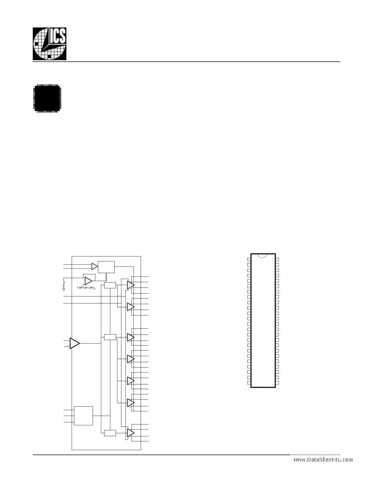
BLOCK DIAGRAM
MULT_0
MULT_1
IREF
PWR_DWN#
SEL_T
-
+
▲
CURRENT
ADJUST
÷1,2,4
PCLK
nPCLK
÷1,2,4
SEL_A
SEL_B
SEL_U
DIVIDER
CONTROL
÷2,4
87158AG
PIN ASSIGNMENT
VDD
HOST_P1
HOST_N1
GND_H
VDD
HOST_P6
HOST_N6
GND_H
VDD
HOST_P2
HOST_N2
GND_H
V
DD
HOST_P3
HOST_N3
GND_H
VDD
HOST_P4
HOST_N4
GND_H
VDD
HOST_P5
HOST_N5
GND_H
GND
VDD
VDD_R
PCLK
nPCLK
GND_R
VDD_M
MREF
nMREF
GND_M
VDD
GND
VDD_L
VDD
GND_L
SEL_T
MULT_0
MULT_1
VDD_L
GND_L
SEL_A
SEL_B
SEL_U
PWR_DWN#
1
2
3
4
5
6
7
8
9
10
11
12
13
14
15
16
17
18
19
20
21
22
23
24
48 VDD
47 GND_H
46 VDD_H
45 HOST_P1
44 HOST_N1
43 GND_H
42 HOST_P2
41 HOST_N2
40 VDD_H
39 HOST_P3
38 HOST_N3
37 GND_H
36 HOST_P4
35 HOST_N4
34 VDD_H
33 HOST_P5
32 HOST_N5
31 GND_H
30 HOST_P6
29 HOST_N6
28 VDD_H
27 IREF
26 GND_I
25 VDD_I
48-Lead TSSOP
6.1mm x 12.5mm x .92mm body package
G Package
Top View
V
DD
MREF
nMREF
GND_H
48-Lead SSOP
7.5mm x 15.9mm x 2.3mm body package
F Package
Top View
www.icst.com/products/hiperclocks.html
REV. B JANUARY 17, 2006
1
1 page 
Integrated
Circuit
Systems, Inc.
ICS87158
1-TO-6, LVPECL-TO-HCSLw/wLwV.DCatMaShOeeSt4U.com
÷1, ÷2, ÷4 CLOCK GENERATOR
TABLE 4D. HCSL DC CHARACTERISTICS, VDD = 3.3V±5%, TA = 0°C TO 85°C
Symbol Parameter
Test Conditions
Minimum Typical
IOH Output Current
12.9
VOH Output High Voltage
RREF = 475Ω, RLOAD = 50Ω
IOH = 6*IREF
0.7
VOL Output Low Voltage
RREF = 475Ω, RLOAD = 50Ω
IOH = 6*IREF
0.03
IOZ High Impedance Leakage Current
-10
VOX Output Crossover Voltage
280
All parameters measured at 200MHz in, 100MHz out on HOST_XX and 50MHz out on MREF.
Current adjust set for VOH = 0.7V. Measurements refer to HOST_XX outputs only.
Maximum Units
14.9 mA
V
V
10 µA
430 mV
TABLE 5A. HCSL AC CHARACTERISTICS, VDD = 3.3V±5%, TA = 0°C TO 85°C
Symbol Parameter
Test Conditions
Minimum Typical Maximum Units
fMAX
tPD
tsk(o)
Output Frequency
Propagation Delay; NOTE 1
Output Skew; NOTE 2, 4, 5
600 MHz
3.7 4.0 ns
60 100 ps
tsk(pp) Part-to-Part Skew; NOTE 3, 5
500 ps
tjit(cc) Cycle-to-Cycle Jitter
150 ps
tR Output Rise Time
tF Output Fall Time
odc Output Duty Cycle
20% to 80%
20% to 80%
175
175
48
700 ps
700 ps
52 %
All parameters measured at 200MHz in, 100MHz out on HOST_XX and 50MHz out on MREF.
Current adjust set for VOH = 0.7V. Measurements refer to HOST_XX outputs only.
NOTE 1: Measured from the differential input crossing point to the differential output crossing point.
NOTE 2: Defined as skew between outputs at the same supply voltage and with equal load conditions.
Measured at the output differential cross points.
NOTE 3: Defined as skew between outputs on different devices operating at the same supply voltages and with equal
load conditions. Using the same type of inputs on each device, the outputs are measured at the differential cross points.
NOTE 4: Maximum value calculated at +3σ from typical.
NOTE 5: This parameter is defined in accordance with JEDEC Standard 65.
TABLE 5B. LVCMOS / LVTTL AC CHARACTERISTICS, VDD = 3.3V±5%, TA = 0°C TO 85°C
Symbol Parameter
Test Conditions
Minimum Typical
fMAX Output Frequency
tjit(cc) Cycle-to-Cycle Jitter
CL = 10pF/30pF
tR Output Rise Time
0.4V to 2.4V, CL = 10pF
0.4V to 2.4V, CL = 30pF
0.4
tF Output Fall Time
0.4V to 2.4V, CL = 10pF
0.4V to 2.4V, C = 30pF
L
0.4
odc Output Duty Cycle
CL = 10pF/30pF
48
All parameters measured at 200MHz in, 100MHz out on HOST_XX and 50MHz out on MREF.
Current adjust set for VOH = 0.7V. Measurements refer to MREF outputs only.
Maximum
300
150
1.8
2
52
Units
MHz
ps
ns
ns
ns
ns
%
87158AG
www.icst.com/products/hiperclocks.html
5
REV. B JANUARY 17, 2006
5 Page 
Integrated
Circuit
Systems, Inc.
ICS87158
1-TO-6, LVPECL-TO-HCSLw/wLwV.DCatMaShOeeSt4U.com
÷1, ÷2, ÷4 CLOCK GENERATOR
Power and Ground
This section provides a layout guide related to power,
ground and placement of bypass capacitors for a high-
speed digital IC. This layout guide is a general recommen-
dation. The actual board design will depend on the compo-
nent types being used, the board density and cost con-
straints. The description assumes that the board has clean
power and ground planes. The principle is to minimize the
ESR between the clean power/ground plane and the IC
power/ground pin.
A low ESR bypass capacitor should be used on each power
pin. The value of bypass capacitors ranges from 0.01uF to
0.1uF. The bypass capacitors should be located as close
to the power pin as possible. It is preferable to locate the
bypass capacitor on the same side as the IC. Figure 4
shows suggested capacitor placement. Placing the by-
pass capacitor on the same side as IC allows the capaci-
tor to have direct contact with the IC power pin. This can
avoid any vias between the bypass capacitor and the IC
power pins.
The vias should be place at the Power/Ground pads. There
should be minimum one via per pin. Increase the number
of vias from the Power/Ground pads to Power/Ground
planes can improve the conductivity.
Power
Pin
C
GND Pin
IC
POWER
Pads
GND
Pads
VIA
FIGURE 4. RECOMMENDED LAYOUT OF BYPASS CAPACITOR PLACEMENT
87158AG
www.icst.com/products/hiperclocks.html
11
REV. B JANUARY 17, 2006
11 Page | ||
| Páginas | Total 16 Páginas | |
| PDF Descargar | [ Datasheet ICS87158.PDF ] | |
Hoja de datos destacado
| Número de pieza | Descripción | Fabricantes |
| ICS87158 | LVPECL-TO-HCSL/LVCMOS | Integrated Circuit Systems |
| Número de pieza | Descripción | Fabricantes |
| SLA6805M | High Voltage 3 phase Motor Driver IC. |
Sanken |
| SDC1742 | 12- and 14-Bit Hybrid Synchro / Resolver-to-Digital Converters. |
Analog Devices |
|
DataSheet.es es una pagina web que funciona como un repositorio de manuales o hoja de datos de muchos de los productos más populares, |
| DataSheet.es | 2020 | Privacy Policy | Contacto | Buscar |