|
|
PDF NCP4303A Data sheet ( Hoja de datos )
| Número de pieza | NCP4303A | |
| Descripción | Secondary Side Synchronous Rectification Driver | |
| Fabricantes | ON Semiconductor | |
| Logotipo | ||
Hay una vista previa y un enlace de descarga de NCP4303A (archivo pdf) en la parte inferior de esta página. Total 26 Páginas | ||
|
No Preview Available !
NCP4303A/B
Secondary Side
Synchronous Rectification
Driver for High Efficiency
SMPS Topologies
The NCP4303A/B is a full featured controller and driver tailored to
control synchronous rectification circuitry in switch mode power
supplies. Thanks to its versatility, it can be used in various topologies
such as flyback, forward and Half Bridge Resonant LLC.
The combination of externally adjustable minimum on and off times
helps to fight the ringing induced by the PCB layout and other
parasitic elements. Therefore, a reliable and noise less operation of the
SR system is insured.
The extremely low turn off delay time, high sink current capability
of the driver and automatic package parasitic inductance
compensation system allow to maximize synchronous rectification
MOSFET conduction time that enables further increase of SMPS
efficiency.
Finally, a wide operating VCC range combined with two versions of
driver voltage clamp eases implementation of the SR system in 24 V
output applications.
Features
• Self−Contained Control of Synchronous Rectifier in CCM, DCM,
and QR Flyback Applications
• Precise True Secondary Zero Current Detection with Adjustable
Threshold
• Automatic Parasitic Inductance Compensation Input
• Typically 40 ns Turn off Delay from Current Sense Input to Driver
• Zero Current Detection Pin Capability up to 200 V
• Ultrafast Trigger Interface to External Signal for CCM operation
• Disable Input to Enter Standby or Low Consumption Mode
• Adjustable Minimum On Time Independent of VCC Level
• Adjustable Minimum Off Time Independent of VCC Level
• 5 A / 2.5 A Peak Current Sink / Source Drive Capability
• Operating Voltage Range up to 30 V
• Gate Drive Clamp of Either 12 V (NCP4303A) or 6 V (NCP4303B)
• Low Startup and Standby Current Consumption
• Maximum Frequency of Operation up to 500 kHz
• SOIC−8 Package
• These are Pb−Free Devices
Typical Applications
• Notebook Adapters
• High Power Density AC/DC Power Supplies
• Gaming Consoles
• All SMPS with High Efficiency Requirements
www.DataSheet4U.com
http://onsemi.com
MARKING
DIAGRAM
8
1
SOIC−8
D SUFFIX
CASE 751
8
XXXXX
ALYWX
G
1
xx = Specific Device Code
A = Assembly Location
WL, L = Wafer Lot
YY, Y = Year
WW, W = Work Week
G or G = Pb−Free Package
PINOUT INFORMATION
VCC
Min_Toff
Min_Ton
Trig/Disable
18
27
36
45
DRV
GND
COMP
CS
ORDERING INFORMATION
Device
Package
Shipping†
NCP4303ADR2G
NCP4303BDR2G
SOIC−8
(Pb−Free)
SOIC−8
(Pb−Free)
2500 /
Tape & Reel
2500 /
Tape & Reel
†For information on tape and reel specifications,
including part orientation and tape sizes, please
refer to our Tape and Reel Packaging Specifications
Brochure, BRD8011/D.
© Semiconductor Components Industries, LLC, 2010
April, 2010 − Rev. 1
1
Publication Order Number:
NCP4303/D
1 page 
NCP4303A/B
ELECTRICAL CHARACTERISTICS (For typical values TJ = 25°C, for min/max values TJ = −40°C to +125°C, Max TJ = 150°C, VCC
= 12 V, Cload = 0
otherwise noted)
nF,
R_min_ton
=
R_min_toff
=
10
kW,
Vtrig
=
0
V,
f_CS
=
100
kHz,
DC_CS
=
50%,
VCS_high
=
4
V,
VCS_low=−w1wVwu.nDleastas Sheet4U.com
Symbol
Rating
Pin Min Typ Max Unit
SUPPLY SECTION
VCC_on
Turn−on threshold level (VCC going up)
VCC_off
Minimum operating voltage after turn−on (VCC going down)
VCC_hyste
VCC hysteresis
ICC1_A
ICC1_B
Internal IC consumption (no output load on pin 8, Fsw = 500 kHz, RTon_min
= RToff_min = 5 kW)
ICC2_A
ICC2_B
Internal IC consumption (Cload = 1 nF on pin 8, Fsw = 400 kHz, RTon_min =
RToff_min = 5 kW)
ICC3_A
ICC3_B
Internal IC consumption (Cload = 10 nF on pin 8, Fsw = 400 kHz, RTon_min =
RToff_min = 5 kW)
ICC_SDM
Startup current consumption (VCC = VCC_on − 0.1 V) and consumption
during light load (disable) mode, (Fsw = 500 kHz, Vtrig = 5 V)
ICC_SDM NS
Startup current consumption (VCC = VCC_on − 0.1 V) and consumption
during light load (disable) mode, (Vcs = 0 V, Vtrig = 5 V)
DRIVE OUTPUT
1
1
1
1
1
1
1
1
9.3 9.9 10.5 V
8.3 8.9 9.5
V
0.8 1.0 1.3
V
− 4.7 − mA
−4−
− 9.3 − mA
− 6.4 −
− 54 − mA
− 34 −
− 390 550 mA
− 280 450 mA
tr_A
tr_B
tf_A
tf_B
Roh
Rol
IDRV_pk(source)
IDRV_pk(sink)
VDRV(H)_A
VDRV(H)_A
VDRV(H)_B
VDRV(H)_B
VDRV(min_A)
VDRV(min_B)
VDRV(CLMP_A)
Output voltage rise−time for A version (Cload = 10 nF), (Note 3)
Output voltage rise−time for B version (Cload = 10 nF), (Note 3)
Output voltage fall−time for A version (Cload = 10 nF), (Note 3)
Output voltage fall−time for B version (Cload = 10 nF), (Note 3)
Driver source resistance (Note 3)
Driver sink resistance
Output source peak current (Note 3)
Output sink peak current (Note 3)
Driver high level output voltage on A version (Cload = 1 nF)
Driver high level output voltage on A version (Cload = 10 nF)
Driver high level output voltage on B version (Cload = 1 nF)
Driver high level output voltage on B version (Cload = 10 nF)
Minimum drive output voltage for A version (VCC = VCC_off + 200 mV)
Minimum drive output voltage for B version (VCC = VCC_off + 200 mV)
Driver clamp voltage for A version, (12 V < VCC < 28 V, minimum Cload =
1 nF)
8
− 120 −
ns
8 − 80 − ns
8 − 50 − ns
8 − 35 − ns
8
− 1.8 7
W
8 − 1 2W
8
− 2.5 −
A
8 −5−A
8 10 − − V
8 11.8 − − V
8 5 −−V
8 6 −−V
8 8.3 − − V
8 4.5 − − V
8 − 12 16 V
VDRV(CLMP_B) Driver clamp voltage for B version, (12 V < VCC < 28 V, minimum Cload = 8 − 7 8.3 V
1 nF)
CS INPUT
Tpd_on
Tpd_off
Ishift_CS
Vth_cs_on
Vth_cs_off
The total propagation delay from CS input to DRV output turn on (VCS goes 5, 8 − 60 90 ns
down from 4 V to −1 V, tf_CS = 5 ns, COMP pin connected to GND)
The total propagation delay from CS input to DRV output turn off (VCS goes 5, 8 − 40 55 ns
up from −1 V to 4 V, tr_CS = 5 ns, COMP pin connected to GND), (Note 3)
Current sense input current source (VCS = 0 V)
Turn on current sense input threshold voltage
5 95 100 105 mA
5, 8 −120 −85 −50 mV
Current sense pin turn off threshold voltage, COMP pin connected to GND
(Note 3)
5, 8
−1
−
0 mV
Gcomp
Compensation inverter gain (Note 3)
3. Guaranteed by design.
5,6,8 − −1 −
−
http://onsemi.com
5
5 Page 
NCP4303A/B
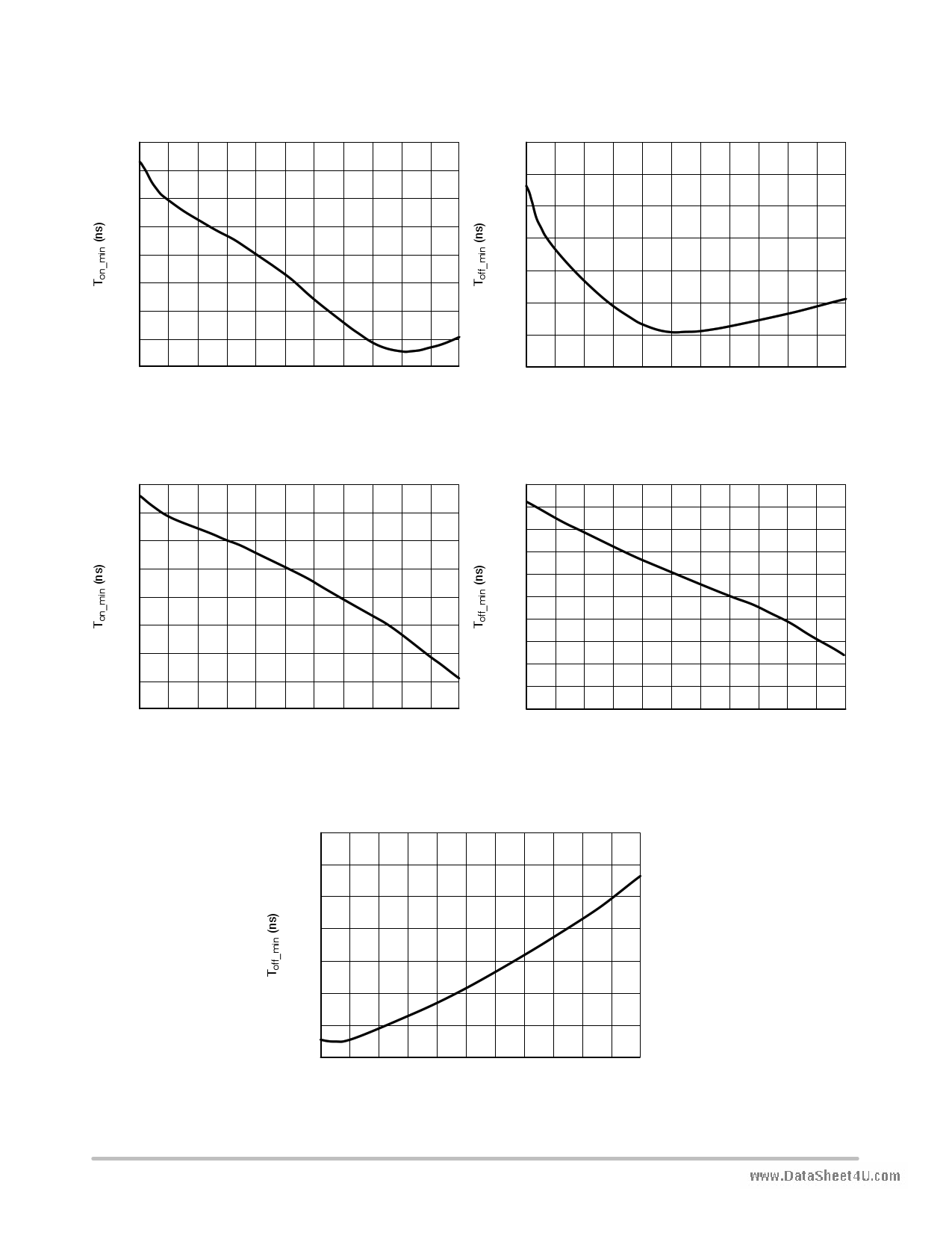
TYPICAL CHARACTERISTICS
1047
www.DataSheet4U.com
976
1046
1045
1044
1043
1042
1041
1040
975
974
973
972
971
970
1039
−40 −25 −10 5 20 35 50 65 80 95 110 125
969
−40 −25 −10 5 20 35 50 65 80 95 110 125
TEMPERATURE (°C)
Figure 28. Minimum on Time @ Rt_on_min =
10 kW
TEMPERATURE (°C)
Figure 29. Minimum Off Time @
Rt_off_min = 10 kW
5340
5320
5300
5280
5260
5240
5220
5200
5180
−40 −25 −10 5 20 35 50 65 80 95
TEMPERATURE (°C)
Figure 30. Minimum on Time @
Rt_on_min = 53 kW
110 125
5050
5000
4950
4900
4850
4800
−40 −25 −10 5 20 35 50 65 80 95
TEMPERATURE (°C)
Figure 31. Minimum Off Time @
Rt_off_min = 53 kW
110 125
640
635
630
625
620
615
610
605
−40 −25 −10 5 20 35 50 65 80 95 110 125
TEMPERATURE (°C)
Figure 32. Minimum Off Time @ Rt_off_min = 0 W
http://onsemi.com
11
11 Page | ||
| Páginas | Total 26 Páginas | |
| PDF Descargar | [ Datasheet NCP4303A.PDF ] | |
Hoja de datos destacado
| Número de pieza | Descripción | Fabricantes |
| NCP4303A | Secondary Side Synchronous Rectification Driver | ON Semiconductor |
| NCP4303B | Secondary Side Synchronous Rectification Driver | ON Semiconductor |
| Número de pieza | Descripción | Fabricantes |
| SLA6805M | High Voltage 3 phase Motor Driver IC. |
Sanken |
| SDC1742 | 12- and 14-Bit Hybrid Synchro / Resolver-to-Digital Converters. |
Analog Devices |
|
DataSheet.es es una pagina web que funciona como un repositorio de manuales o hoja de datos de muchos de los productos más populares, |
| DataSheet.es | 2020 | Privacy Policy | Contacto | Buscar |
