|
|
|
PDF DS42BR400 Data sheet ( Hoja de datos )
| Número de pieza | DS42BR400 | |
| Descripción | Quad 4.25 Gbps CML Transceiver | |
| Fabricantes | National Semiconductor | |
| Logotipo | ||
Hay una vista previa y un enlace de descarga de DS42BR400 (archivo pdf) en la parte inferior de esta página. Total 14 Páginas | ||
|
No Preview Available !
March 27, 2008
DS42BR400
Quad 4.25 Gbps CML Transceiver with Transmit
De-Emphasis and Receive Equalization
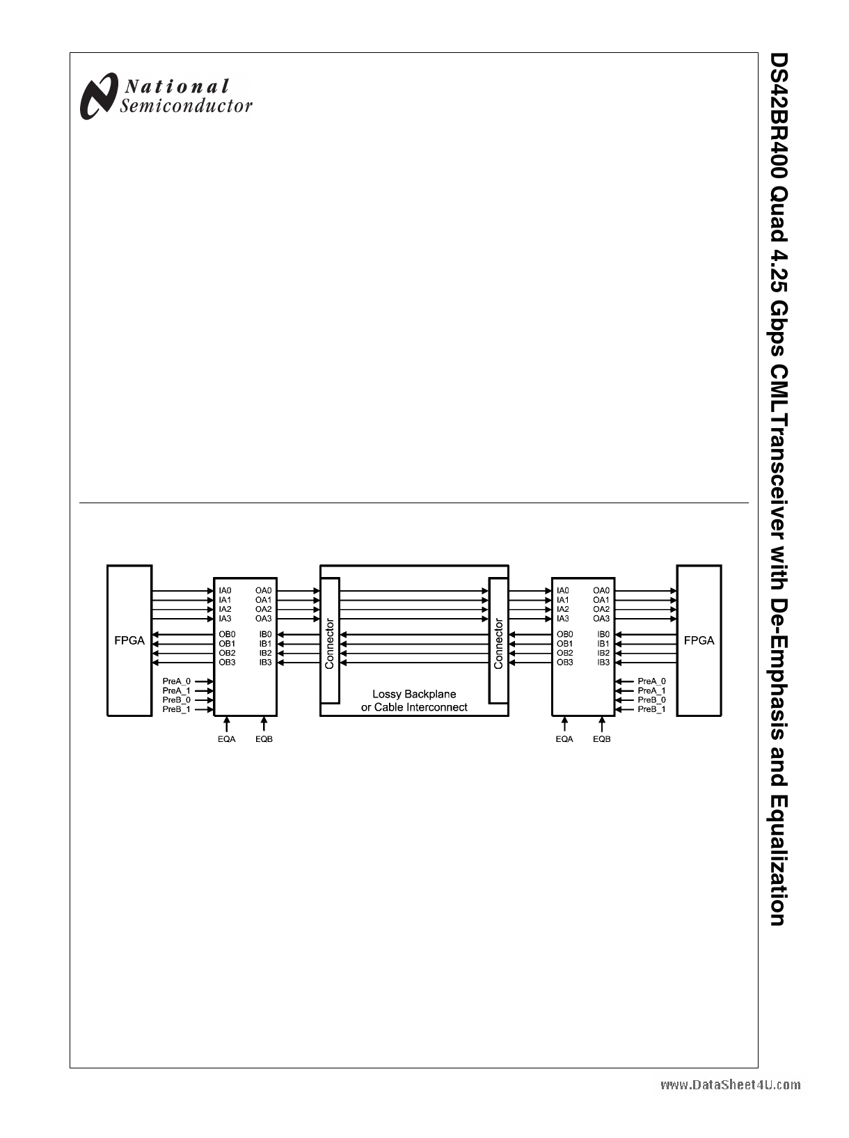
General Description
The DS42BR400 is a quad 250 Mbps – 4.25 Gbps CML
transceiver, or 8-channel buffer, for use in backplane and ca-
ble applications. With operation down to 250 Mbps, the
DS42BR400 can be used in applications requiring both low
and high frequency data rates. Each input stage has a fixed
equalizer to reduce ISI distortion from board traces. The
equalizers are grouped in fours and are enabled through two
www.DcaotnatSrohlepeint4sU. .Tchoemse control pins provide customers flexibility
where ISI distortion may vary from one direction to another.
All output drivers have four selectable steps of de-emphasis
to compensate against transmission loss across long FR4
backplanes. The de-emphasis blocks are also grouped in
fours. In addition, the DS42BR400 also has loopback control
capability on four channels. All CML drivers have 50Ω termi-
nation to VCC. All receivers are internally terminated with
differential 100Ω.
Features
■ 250 Mbps – 4.25 Gbps Fully Differential Data Paths
■ Optional Fixed Input Equalization
■ Selectable Output De-emphasis
■ Individual Loopback Controls
■ On-chip Termination
■ Lead-less eLLP-60 pin package (9 mm x 9 mm x 0.8 mm,
0.5 mm pitch)
■ −40°C to +85°C Industrial Temperature Range
■ 6 kV ESD Rating, HBM
Applications
■ Backplane driver or cable driver
■ Signal repeating, buffering and conditioning applications
Simplified Application Diagram
20182440
© 2008 National Semiconductor Corporation 201824
www.national.com
1 page 
Pin Name Pin Number I/O
CONTROL (3.3V LVCMOS)
EQA
60 I
EQB
16 I
PreA_0
PreA_1
PreB_0
PreB_1
LB0
15 I
1
31 I
45
46 I
LB1 44 I
LB2 32 I
LwBw3w.DataSheet4U3.0com I
RSV
59 I
POWER
VCC
5, 11, 20, 26,
35, 41, 50,
56
P
GND
GND
2, 8, 14, 17,
23, 29, 38,
47, 53
DAP
P
P
Description
This pin is active LOW. A logic LOW at EQA enables equalization for input channels IA_0±, IA_1±,
IA_2±, and IA_3±. By default, this pin is internally pulled high and equalization is disabled.
This pin is active LOW. A logic LOW at EQB enables equalization for input channels IB_0±, IB_1±,
IB_2±, and IB_3±. By default, this pin is internally pulled high and equalization is disabled.
PreA_0 and PreA_1 select the output de-emphasis levels (OA_0±, OA_1±, OA_2±, and OA_3±).
PreA_0 and PreA_1 are internally pulled high. Please see Table 2 for de-emphasis levels.
PreB_0 and PreB_1 select the output de-emphasis levels (OB_0±, OB_1±, OB_2±, and OB_3±).
PreB_0 and PreB_1 are internally pulled high. Please see Table 2 for de-emphasis levels.
This pin is active LOW. A logic LOW at LB0 enables the internal loopback path from IB_0± to OA_0
±. LB0 is internally pulled high. Please see Table 1 for more information.
This pin is active LOW. A logic LOW at LB1 enables the internal loopback path from IB_1± to OA_1
±. LB1 is internally pulled high. Please see Table 1 for more information.
This pin is active LOW. A logic LOW at LB2 enables the internal loopback path from IB_2± to OA_2
±. LB2 is internally pulled high. Please see Table 1 for more information.
This pin is active LOW. A logic LOW at LB3 enables the internal loopback path from IB_3± to OA_3
±. LB3 is internally pulled high. Please see Table 1 for more information.
Reserve pin to support factory testing. This pin can be left open, tied to GND, or tied to GND through
an external pull-down resistor.
VCC = 3.3V ± 5%.
Each VCC pin should be connected to the VCC plane through a low inductance path, typically with a
via located as close as possible to the landing pad of the VCC pin.
It is recommended to have a 0.01 μF or 0.1 μF, X7R, size-0402 bypass capacitor from each VCC
pin to ground plane.
Ground reference. Each ground pin should be connected to the ground plane through a low
inductance path, typically with a via located as close as possible to the landing pad of the GND pin.
DAP is the metal contact at the bottom side, located at the center of the eLLP-60 pin package. It
should be connected to the GND plane with at least 4 via to lower the ground impedance and
improve the thermal performance of the package.
Note: I = Input, O = Output, P = Power
5 www.national.com
5 Page 
Timing Diagrams
20182436
FIGURE 2. Driver Output Transition Time
www.DataSheet4U.com
FIGURE 3. Propagation Delay
20182435
FIGURE 4. Loopback Delay Timing
20182403
11 www.national.com
11 Page | ||
| Páginas | Total 14 Páginas | |
| PDF Descargar | [ Datasheet DS42BR400.PDF ] | |
Hoja de datos destacado
| Número de pieza | Descripción | Fabricantes |
| DS42BR400 | DS42BR400 Quad 4.25Gbps CML Transcvr w/Transmit De-Emphasis Recve Equal (Rev. J) | Texas Instruments |
| DS42BR400 | Quad 4.25 Gbps CML Transceiver | National Semiconductor |
| Número de pieza | Descripción | Fabricantes |
| SLA6805M | High Voltage 3 phase Motor Driver IC. |
Sanken |
| SDC1742 | 12- and 14-Bit Hybrid Synchro / Resolver-to-Digital Converters. |
Analog Devices |
|
DataSheet.es es una pagina web que funciona como un repositorio de manuales o hoja de datos de muchos de los productos más populares, |
| DataSheet.es | 2020 | Privacy Policy | Contacto | Buscar |