|
|
PDF W3H32M72E-XSBX Data sheet ( Hoja de datos )
| Número de pieza | W3H32M72E-XSBX | |
| Descripción | 32M x 72 DDR2 SDRAM 208 PBGA Multi-Chip Package | |
| Fabricantes | White Electronic Designs | |
| Logotipo |  |
|
Hay una vista previa y un enlace de descarga de W3H32M72E-XSBX (archivo pdf) en la parte inferior de esta página. Total 30 Páginas | ||
|
No Preview Available !
White Electronic Designs
W3H32M72E-XSBX
PRELIMINARY*
32M x 72 DDR2 SDRAM 208 PBGA Multi-Chip Package
FEATURES
Data rate = 667*, 533, 400
Programmable CAS latency: 3, 4, 5, or 6
Package:
Posted CAS additive latency: 0, 1, 2, 3 or 4
• 208 Plastic Ball Grid Array (PBGA), 18 x 20mm
Write latency = Read latency - 1* tCK
• 1.0mm pitch
wwwD.DiffaetraeSnhtieael td4aUt.acostmrobe (DQS, DQS#) per byte
Internal, pipelined, double data rate architecture
4-bit prefetch architecture
Commercial, Industrial and Military Temperature
Ranges
Organized as 32M x 72
Weight: W3H32M72E-XSBX - 2.5 grams typical
DLL for alignment of DQ and DQS transitions with
clock signal
Four internal banks for concurrent operation
(Per DDR2 SDRAM Die)
Programmable Burst lengths: 4 or 8
Auto Refresh and Self Refresh Modes
On Die Termination (ODT)
Adjustable data – output drive strength
Single 1.8V ±0.1V supply
BENEFITS
65% SPACE SAVINGS vs. FPBGA
Reduced part count
54% I/O reduction vs FPBGA
Reduced trace lengths for lower parasitic
capacitance
Suitable for hi-reliability applications
Upgradable to 64M x 72 density (contact factory for
information)
* This product is under development, is not qualified or characterized and is subject
to change without notice.
11.0
90
19.0 FBGA
FIGURE 1 – DENSITY COMPARISONS
CSP Approach (mm)
11.0 11.0 11.0
11.0
90
FBGA
90
FBGA
90
FBGA
90
FBGA
Actual Size
W3H32M72E-XSBX
White Electronic Designs
W3H32M72E-XSBX
20
18
S
A
V
I
N
G
S
Area
I/O
Count
5 x 209mm2 = 1,045mm2
5 x 90 balls = 450 balls
360mm2
208 Balls
65%
54%
White Electronic Designs Corp. reserves the right to change products or specifications without notice.
February 2006
Rev. 2
1 White Electronic Designs Corporation • (602) 437-1520 • www.wedc.com
1 page 
White Electronic Designs
W3H32M72E-XSBX
PRELIMINARY*
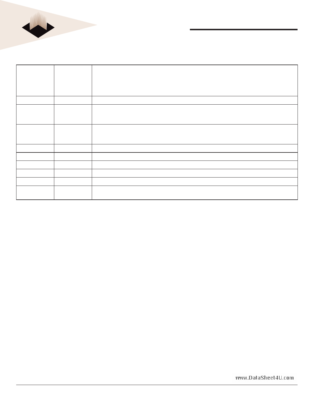
A0-A12
Input
DQ0-71
I/O
wwUDwQ.SD,aUtDaQSSh#eet4U.comI/O
LDQS, LDQS#
VCC
VCCQ
VREF
VSS
NC
DNU
I/O
Supply
Supply
Supply
Supply
-
-
TABLE – 1 BALL DESCRIPTIONS (continued)
Address inputs: Provide the row address for ACTIVE commands, and the column address and auto precharge bit
(A10) for READ/WRITE commands, to select one location out of the memory array in the respective bank. A10
sampled during a PRECHARGE command determines whether the PRECHARGE applies to one bank (A10 LOW,
bank selected by BA1–BA0) or all banks (A10 HIGH) The address inputs also provide the op-code during a LOAD
MODE command.
Data input/output: Bidirectional data bus
Data strobe for upper byte: Output with read data, input with write data for source synchronous operation. Edge-
aligned with read data, center-aligned with write data. UDQS# is only used when differential data strobe mode is
enabled via the LOAD MODE command.
Data strobe for lower byte: Output with read data, input with write data for source synchronous operation. Edge-
aligned with read data, center-aligned with write data. UDQS# is only used when differential data strobe mode is
enabled via the LOAD MODE command.
Power Supply: 1.8V ±0.1V
DQ Power supply: 1.8V ±0.1V. Isolated on the device for improved noise immunity
SSTL_18 reference voltage.
Ground
No connect: These balls should be left unconnected.
Future use; Row address bits A14 and A15 are reserved for 8Gb and 16Gb densities. BA2 is reserved for 4Gb
device.
White Electronic Designs Corp. reserves the right to change products or specifications without notice.
February 2006
Rev. 2
5 White Electronic Designs Corporation • (602) 437-1520 • www.wedc.com
5 Page 
White Electronic Designs
W3H32M72E-XSBX
PRELIMINARY*
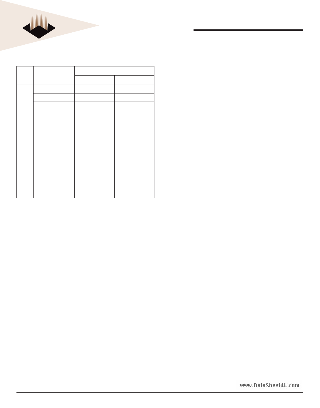
TABLE 2 – BURST DEFINITION
Burst Starting Column
Length
Address
Order of Accesses Within a Burst
Type = Sequential Type = Interleaved
A1 A0
00
4 01
10
www.DataSheet4U.com
11
0-1-2-3
1-2-3-0
2-3-0-1
3-0-1-2
0-1-2-3
1-0-3-2
2-3-0-1
3-2-1-0
A2 A1 A0
0 0 0 0-1-2-3-4-5-6-7
0 0 1 1-2-3-4-5-6-7-0
0 1 0 2-3-4-5-6-7-0-1
8 0 1 1 3-4-5-6-7-0-1-2
1 0 0 4-5-6-7-0-1-2-3
1 0 1 5-6-7-0-1-2-3-4
1 1 0 6-7-0-1-2-3-4-5
1 1 1 7-0-1-2-3-4-5-6
0-1-2-3-4-5-6-7
1-0-3-2-5-4-7-6
2-3-0-1-6-7-4-5
3-2-1-0-7-6-5-4
4-5-6-7-0-1-2-3
5-4-7-6-1-0-3-2
6-7-4-5-2-3-0-1
7-6-5-4-3-2-1-0
NOTES:
1. For a burst length of two, A1-Ai select two-data-element block; A0 selects the
starting column within the block.
2. For a burst length of four, A2-Ai select four-data-element block; A0-1 select the
starting column within the block.
3. For a burst length of eight, A3-Ai select eight-data-element block; A0-2 select the
starting column within the block.
4. Whenever a boundary of the block is reached within a given sequence above, the
following access wraps within the block.
OPERATING MODE
The normal operating mode is selected by issuing a
command with bit M7 set to “0,” and all other bits set to
the desired values, as shown in Figure 5. When bit M7 is
“1,” no other bits of the mode register are programmed.
Programming bit M7 to “1” places the DDR2 SDRAM into a
test mode that is only used by the manufacturer and should
not be used. No operation or functionality is guaranteed
if M7 bit is ‘1.’
DLL RESET
DLL RESET is defined by bit M8, as shown in Figure 5.
Programming bit M8 to “1” will activate the DLL RESET
function. Bit M8 is self-clearing, meaning it returns back
to a value of “0” after the DLL RESET function has been
issued.
Anytime the DLL RESET function is used, 200 clock cycles
must occur before a READ command can be issued to
allow time for the internal clock to be synchronized with
the external clock. Failing to wait for synchronization
to occur may result in a violation of the tAC or tDQSCK
parameters.
WRITE RECOVERY
Write recovery (WR) time is defined by bits M9–M11, as
shown in Figure 5. The WR register is used by the DDR2
SDRAM during WRITE with auto precharge operation.
During WRITE with auto precharge operation, the DDR2
SDRAM delays the internal auto precharge operation by
WR clocks (programmed in bits M9–M11) from the last
data burst.
WR values of 2, 3, 4, 5, or 6 clocks may be used for
programming bits M9–M11. The user is required to
program the value of WR, which is calculated by dividing
tWR (in ns) by tCK (in ns) and rounding up a non integer
value to the next integer; WR [cycles] = tWR [ns] / tCK [ns].
Reserved states should not be used as unknown operation
or incompatibility with future versions may result.
POWER-DOWN MODE
Active power-down (PD) mode is defined by bit M12,
as shown in Figure 5. PD mode allows the user to
determine the active power-down mode, which determines
performance versus power savings. PD mode bit M12 does
not apply to precharge PD mode.
When bit M12 = 0, standard active PD mode or “fast-exit”
active PD mode is enabled. The tXARD parameter is used
for fast-exit active PD exit timing. The DLL is expected to
be enabled and running during this mode.
When bit M12 = 1, a lower-power active PD mode or “slow-
exit” active PD mode is enabled. The tXARD parameter is
used for slow-exit active PD exit timing. The DLL can be
enabled, but “frozen” during active PD mode since the exit-
to-READ command timing is relaxed. The power difference
expected between PD normal and PD low-power mode is
defined in the ICC table.
White Electronic Designs Corp. reserves the right to change products or specifications without notice.
February 2006
Rev. 2
11 White Electronic Designs Corporation • (602) 437-1520 • www.wedc.com
11 Page | ||
| Páginas | Total 30 Páginas | |
| PDF Descargar | [ Datasheet W3H32M72E-XSBX.PDF ] | |
Hoja de datos destacado
| Número de pieza | Descripción | Fabricantes |
| W3H32M72E-XSBX | 32M x 72 DDR2 SDRAM 208 PBGA Multi-Chip Package | White Electronic Designs |
| Número de pieza | Descripción | Fabricantes |
| SLA6805M | High Voltage 3 phase Motor Driver IC. |
Sanken |
| SDC1742 | 12- and 14-Bit Hybrid Synchro / Resolver-to-Digital Converters. |
Analog Devices |
|
DataSheet.es es una pagina web que funciona como un repositorio de manuales o hoja de datos de muchos de los productos más populares, |
| DataSheet.es | 2020 | Privacy Policy | Contacto | Buscar |
