|
|
|
PDF ICS8624 Data sheet ( Hoja de datos )
| Número de pieza | ICS8624 | |
| Descripción | 1-TO-5 DIFFERENTIAL-TO-HSTL ZERO DELAY BUFFER | |
| Fabricantes | Integrated Circuit Systems | |
| Logotipo | ||
Hay una vista previa y un enlace de descarga de ICS8624 (archivo pdf) en la parte inferior de esta página. Total 16 Páginas | ||
|
No Preview Available !
Integrated
Circuit
Systems, Inc.
ICS8624
LOW SKEW, 1-TO-5
DIFFERENTIAL-TO-HSTL ZERO DELAY BUFFER
GENERAL DESCRIPTION
ICS
The ICS8624 is a high performance, 1-to-5
Differential-to-HSTL zero delay buffer and
HiPerClockS™ a member of the HiPerClockS™ family of High
Performance Clock Solutions from ICS. The
ICS8624 has two selectable clock input pairs.
The CLK0, nCLK0 and CLK1, nCLK1 pair can accept most
standard differential input levels. The VCO operates at a fre-
quency range of 250MHz to 700MHz. Utilizing one of the
outputs as feedback to the PLL, output frequencies up to
700MHz can be regenerated with zero delay with respect to
www.DthaetainShpeuet.tD4Uu.aclormeference clock inputs support redundant clock
or multiple reference applications.
FEATURES
• Fully integrated PLL
• 5 differential HSTL outputs
• Selectable differential CLKx, nCLKx input pairs
• CLKx, nCLKx pairs can accept the following differential
input levels: LVPECL, LVDS, HSTL, SSTL, HCSL
• Output frequency range: 31.25MHz to 700MHz
• Input frequency range: 31.25MHz to 700MHz
• VCO range: 250MHz to 700MHz
• External feedback for “zero delay” clock regeneration
• Cycle-to-cycle jitter: 25ps (maximum)
• Output skew: 25ps (maximum)
• Static phase offset: ±100ps
• 3.3V core, 1.8V output operating supply
• 0°C to 70°C ambient operating temperature
• Lead-Free package available
• Industrial temperature information available upon request
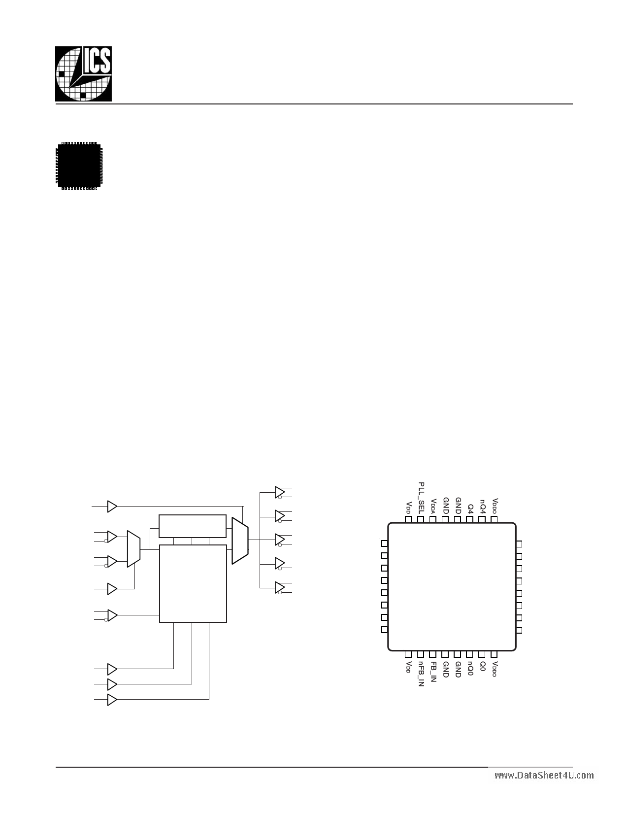
BLOCK DIAGRAM
PLL_SEL
CLK0
nCLK0
CLK1
nCLK1
CLK_SEL
FB_IN
nFB_IN
0
1
÷4, ÷8
PLL
0
1
SEL0
SEL1
MR
PIN ASSIGNMENT
Q0
nQ0
Q1
nQ1
Q2
nQ2
SEL0
32 31 30 29 28 27 26 25
1 24
VDDO
Q3
nQ3
SEL1 2
CLK0 3
23 Q3
22 nQ3
Q4
nQ4
nCLK0 4
CLK1 5
ICS8624
21 Q2
20 nQ2
nCLK1 6
19 Q1
CLK_SEL 7
18 nQ1
MR 8
1 7 VDDO
9 10 11 12 13 14 15 16
32-Lead LQFP
7mm x 7mm x 1.4mm body package
Y Package
Top View
8624BY
www.icst.com/products/hiperclocks.html
1
REV. C JUNE 15, 2004
1 page 
Integrated
Circuit
Systems, Inc.
ICS8624
LOW SKEW, 1-TO-5
DIFFERENTIAL-TO-HSTL ZERO DELAY BUFFER
TABLE 4D. HSTL DC CHARACTERISTICS, VDD = VDDA = 3.3V±5%, VDDO = 1.8V±0.2V, TA = 0°C TO 70°C
Symbol Parameter
Test Conditions
Minimum Typical
VOH Output High Voltage; NOTE 1
VOL Output Low Voltage; NOTE 1
VOX Output Crossover Voltage; NOTE 2
VSWING Peak-to-Peak Output Voltage Swing
NOTE 1: Outputs terminated with 50Ω to ground.
NOTE 2: Defined with respect to output voltage swing at a given condition.
1.0
0
40
0.6
Maximum
1.4
0.4
60
1.1
Units
V
V
%
V
www.DataSheet4U.com
TABLE
5.
INPUT
FREQUENCY
CHARACTERISTICS,
V
DD
=
V
DDA
=
3.3V±5%,
V
DDO
=
1.8V±0.2V,
TA
=
0°C
TO
70°C
Symbol
fIN
Parameter
Input Frequency
CLK0, nCLK0,
CLK1, nCLK1
Test Conditions
PLL_SEL = 1
PLL_SEL = 0
Minimum
31.25
Typical
Maximum
700
700
Units
MHz
MHz
TABLE 6A. AC CHARACTERISTICS, VDD = VDDA = 3.3V±5%, VDDO = 1.8V±0.2V, TA = 0°C TO 70°C
Symbol Parameter
Test Conditions
Minimum Typical Maximum
fMAX Output Frequency
tPD Propagation Delay; NOTE 1
t(Ø) Static Phase Offset; NOTE 2, 5
IJ 700MHz
PLL_SEL = 3.3V
3.4
-100
3.9
700
4.4
100
tsk(o) Output Skew; NOTE 3, 5
25
tjit(cc)
tjit(Ø)
Cycle-to-Cycle Jitter; NOTE 5, 6
Phase Jitter; NOTE 4, 5, 6
25
±50
t PLL Lock Time
L
1
tR Output Rise Time
20% to 80% @ 50MHz
300
700
tF Output Fall Time
20% to 80% @ 50MHz
300
700
tPW Output Pulse Width
tcycle/2 - 85 tcycle/2 tcycle/2 + 85
All parameters measured at f unless noted otherwise.
MAX
NOTE 1: Measured from the differential input crossing point to the differential output crossing point.
NOTE 2: Defined as the time difference between the input reference clock and the averaged feedback input signal
across all conditions, when the PLL is locked and the input reference frequency is stable.
NOTE 3: Defined as skew between outputs at the same supply voltage and with equal load conditions.
Measured at output differential cross points.
NOTE 4: Phase jitter is dependent on the input source used.
NOTE 5: This parameter is defined in accordance with JEDEC Standard 65.
NOTE 6: Characterized at VCO frequency of 622MHz.
Units
MHz
ns
ps
ps
ps
ps
ms
ps
ps
ps
TABLE 6B. AC CHARACTERISTICS, VDD = VDDA = 3.3V±10%, VDDO = 1.8V±0.2V, TA = 0°C TO 70°C
Symbol Parameter
Test Conditions
Minimum Typical
tjit(cc) Cycle-to-Cycle Jitter; NOTE 1
NOTE 1: This parameter is defined in accordance with JEDEC Standard 65.
Maximum
35
Units
ps
8624BY
www.icst.com/products/hiperclocks.html
5
REV. C JUNE 15, 2004
5 Page 
Integrated
Circuit
Systems, Inc.
ICS8624
LOW SKEW, 1-TO-5
DIFFERENTIAL-TO-HSTL ZERO DELAY BUFFER
POWER CONSIDERATIONS
This section provides information on power dissipation and junction temperature for the ICS8624.
Equations and example calculations are also provided.
1. Power Dissipation.
The total power dissipation for the ICS8624 is the sum of the core power plus the power dissipated in the load(s).
The following is the power dissipation for VDD = 3.3V + 5% = 3.465V, which gives worst case results.
NOTE: Please refer to Section 3 for details on calculating power dissipated in the load.
www.DataS•heetP4oUw.ceorm(core)MAX = VDD_MAX * IDD_MAX = 3.465V * 120mA = 416mW
• Power (outputs)MAX = 32.8mW/Loaded Output pair
If all outputs are loaded, the total power is 5 * 32.8mW = 164mW
Total Power_MAX (3.465V, with all outputs switching) = 416mW + 164mW = 580mW
2. Junction Temperature.
Junction temperature, Tj, is the temperature at the junction of the bond wire and bond pad and directly affects the reliability of the
device.The maximum recommended junction temperature for HiPerClockSTM devices is 125°C.
The equation for Tj is as follows: Tj = θJA * Pd_total + TA
Tj = Junction Temperature
θJA = Junction-to-Ambient Thermal Resistance
Pd_total = Total Device Power Dissipation (example calculation is in section 1 above)
TA = Ambient Temperature
In order to calculate junction temperature, the appropriate junction-to-ambient thermal resistance θJA must be used. Assuming a
moderate air flow of 200 linear feet per minute and a multi-layer board, the appropriate value is 42.1°C/W per Table 7 below.
Therefore, Tj for an ambient temperature of 70°C with all outputs switching is:
70°C + 0.580W * 42.1°C/W = 94.4°C. This is well below the limit of 125°C.
This calculation is only an example. Tj will obviously vary depending on the number of loaded outputs, supply voltage, air flow,
and the type of board (single layer or multi-layer).
TABLE 7. THERMAL RESISTANCE θJA FOR 32-PIN LQFP, FORCED CONVECTION
θJA by Velocity (Linear Feet per Minute)
Single-Layer PCB, JEDEC Standard Test Boards
Multi-Layer PCB, JEDEC Standard Test Boards
0
67.8°C/W
47.9°C/W
200
55.9°C/W
42.1°C/W
500
50.1°C/W
39.4°C/W
NOTE: Most modern PCB designs use multi-layered boards.The data in the second row pertains to most designs.
8624BY
www.icst.com/products/hiperclocks.html
11
REV. C JUNE 15, 2004
11 Page | ||
| Páginas | Total 16 Páginas | |
| PDF Descargar | [ Datasheet ICS8624.PDF ] | |
Hoja de datos destacado
| Número de pieza | Descripción | Fabricantes |
| ICS8624 | 1-TO-5 DIFFERENTIAL-TO-HSTL ZERO DELAY BUFFER | Integrated Circuit Systems |
| Número de pieza | Descripción | Fabricantes |
| SLA6805M | High Voltage 3 phase Motor Driver IC. |
Sanken |
| SDC1742 | 12- and 14-Bit Hybrid Synchro / Resolver-to-Digital Converters. |
Analog Devices |
|
DataSheet.es es una pagina web que funciona como un repositorio de manuales o hoja de datos de muchos de los productos más populares, |
| DataSheet.es | 2020 | Privacy Policy | Contacto | Buscar |