|
|
|
PDF NB4N1158 Data sheet ( Hoja de datos )
| Número de pieza | NB4N1158 | |
| Descripción | Link Replicator | |
| Fabricantes | ON Semiconductor | |
| Logotipo | ||
Hay una vista previa y un enlace de descarga de NB4N1158 (archivo pdf) en la parte inferior de esta página. Total 8 Páginas | ||
|
No Preview Available !
NB4N1158
Link Replicator for Fibre
Channel, Gigabit Ethernet,
HDTV and SATA
Up to 1.5 Gb/s
Description
The NB4N1158 is a high performance 3.3 V Serial Link Replicator
which provides the function of serial loop replication and serial
loopback control commonly required in Fibre Channel, GbE, HDTV
and SATA applications. Other popular applications include Host Bus
www.DaAtadSahpetoert4sUf.ocromrouting between internal and external connectors, and
hot-pluggable links between redundant switch fabric cards.
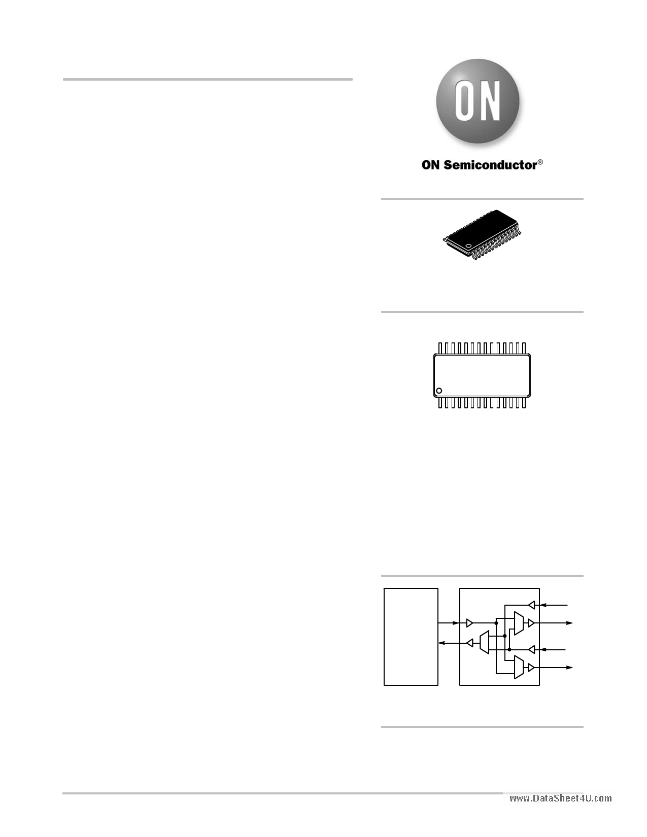
IN is sent to both OUT0 and OUT1; each output is enabled by OE0
and OE1 when HIGH. OUT0 can select either IN or IN1 via the
MUX0 pin. Likewise, OUT1 can select between IN or IN0 via the
MUX1 pin. Out can select between IN0 and IN1.
In Link Replicator applications, such as the Line Card to Switch
Card links, IN is transmitted to both OUT0 and OUT1 which either
IN0 or IN1 is selected at OUT. In Host Adapter applications, IN goes
to OUT0 (an internal connector) which returns data on IN0. IN0 is
looped to OUT1 (an external connector) which returns data on IN1 and
then back to the SerDes on OUT.
The NB4N1158 is packaged in a 4.7 mm x 9.7 mm TSSOP-28.
Features
•ăReplicates Fibre Channel, Gigabit Ethernet, HDTV, and
Serial ATA (SATA) Links
•ăT11 Fibre Channel Complaint at 1.0625 Gb/s
•ăDifferential LVPECL Outputs, External Load/Termination
Resistors Required
•ăIEEE802.3z Gigabit Ethernet Compliant at 1.25 Gb/s
•ăSMPTE-292M Compliant at 1.485 Gb/s
•ă330 mW Maximum Power Dissipation
•ăOperating Range: VCC = 3.135 V to 3.465 V
•ă28-pin, 4.4 mm x 9.7 mm TSSOP Package
•ăThese are Pb-Free Devices
http://onsemi.com
28 Lead TSSOP
DT SUFFIX
CASE 948A
MARKING DIAGRAM*
NB4N
1158
ALYW
A = Assembly Location
L = Wafer Lot
Y = Year
W = Work Week
G or G = Pb-Free Package
(Note: Microdot may be in either location)
*For additional marking information, refer to
Application Note AND8002/D.
NB4N1158
LOOP0
TX
RX
LOOP1
©Ă Semiconductor Components Industries, LLC, 2007
December, 2007 - Rev. 0
Figure 1. Simplified Application
ORDERING INFORMATION
See detailed ordering and shipping information in the package
dimensions section on page 6 of this data sheet.
1 Publication Order Number:
NB4N1158/D
1 page 
NB4N1158
0.01mF
TX+ I+
R
0.01mF
RT
TX-
R
I-
0.01mF
O1+ I1+
R
0.01mF
RT
O1-
R
I1-
0.01mF
O+ RX+
R
0.01mF
RT
O-
R
RX-
SerDes
RX+
RX-
www.DataSheet4U.com
0.01mF
RT
0.01mF
NB4N1158
O+
R
O-
R
I1+
I1-
0.01mF
RT R
0.01mF
R
NB4N1158
O1+ I+
O1- I-
0.01mF
RT R
0.01mF
R
“R” is 150 W for both 100 W differential or 150 W differential traces.
“RT” matches the differential impedance of the link.
SerDes
TX+
TX-
Figure 5. NB4N1158 Application Interface Example
IN+/IN- Input Functionality
The differential inputs are internally biased to Y1.2 V. In
a typical application, the differential inputs are
capacitor-coupled and will swing symmetrically above and
below 1.2 V, preserving a 50% duty cycle to the outputs.
With this technique, the NB4N1158 will accept any
differential input allowing for LVPECL, CML, LVDS, and
HSTL input levels.
OUT+ / OUT- Outputs
The differential output buffers of the NB4N1158 utilize
standard Positive Emitter Coupled Logic (PECL)
architecture for OUT+ and OUT-. The outputs are designed
to drive differential transmission lines with nominally 50 W
or 75 W characteristic impedance. External
DC load/termination with a 50 W resistor to VTT = VDD -
2.0 V is required. See Figure 6 for output termination
scheme.
OEx Output Enable
The NB4N1158 incorporates output enable pins, OE0 and
OE1, that work by powering down the output buffer and
associated driving circuitry. Using this approach results in
both differential outputs going HIGH, and a reduction in IDD
current of approx. 29 mA for each disabled output pair.
When OEx is LOW, outputs are disabled, OUTx+ and
OUTx- are set HIGH.
Power Supply Bypass information
A clean power supply will optimize the performance of
the device. The NB4N1158 provides separate power supply
pins for the digital circuitry (VDD) and LVPECL outputs
(VDDPn). Placing a bypass capacitor of 0.01 mF to 0.1 mF
on each VDD pin will help ensure a noise free VDD power
supply. The purpose of this design technique is to try and
isolate the high switching noise of the digital outputs from
the relatively sensitive digital core logic.
Driver
Device
Q
Q
Zo = 50 W
Zo = 50 W
50 W
50 W
D
Receiver
Device
D
VTT
VTT = VCC - 2.0 V
Figure 6. Typical Termination for Output Driver and Device Evaluation
(See Application Note AND8020/D - Termination of ECL Logic Devices.)
http://onsemi.com
5
5 Page | ||
| Páginas | Total 8 Páginas | |
| PDF Descargar | [ Datasheet NB4N1158.PDF ] | |
Hoja de datos destacado
| Número de pieza | Descripción | Fabricantes |
| NB4N1158 | Link Replicator | ON Semiconductor |
| Número de pieza | Descripción | Fabricantes |
| SLA6805M | High Voltage 3 phase Motor Driver IC. |
Sanken |
| SDC1742 | 12- and 14-Bit Hybrid Synchro / Resolver-to-Digital Converters. |
Analog Devices |
|
DataSheet.es es una pagina web que funciona como un repositorio de manuales o hoja de datos de muchos de los productos más populares, |
| DataSheet.es | 2020 | Privacy Policy | Contacto | Buscar |