|
|
|
PDF ADC122S051 Data sheet ( Hoja de datos )
| Número de pieza | ADC122S051 | |
| Descripción | 2 Channel- 500 kSPS 12-Bit A/D Converter | |
| Fabricantes | National Semiconductor | |
| Logotipo | ||
Hay una vista previa y un enlace de descarga de ADC122S051 (archivo pdf) en la parte inferior de esta página. Total 19 Páginas | ||
|
No Preview Available !
April 2005
www.DataSheet4U.com
ADC122S051
2 Channel, 500 kSPS 12-Bit A/D Converter
General Description
The ADC122S051 is a low-power, two-channel CMOS 12-bit
analog-to-digital converter with a high-speed serial interface.
Unlike the conventional practice of specifying performance
at a single sample rate only, the ADC122S051 is fully speci-
fied over a sample rate range of 200 kSPS to 500 kSPS. The
converter is based on a successive-approximation register
architecture with an internal track-and-hold circuit. It can be
configured to accept one or two input signals at inputs IN1
and IN2.
The output serial data is straight binary, and is compatible
with several standards, such as SPI™, QSPI™, MICROW-
IRE, and many common DSP serial interfaces.
The ADC122S051 operates with a single supply that can
range from +2.7V to +5.25V. Normal power consumption
using a +3V or +5V supply is 3.0 mW and 10 mW, respec-
tively. The power-down feature reduces the power consump-
tion to just 0.14 µW using a +3V supply, or 0.32 µW using a
+5V supply.
The ADC122S051 is packaged in an 8-lead MSOP package.
Operation over the industrial temperature range of −40˚C to
+85˚C is guaranteed.
Features
n Specified over a range of sample rates.
n Two input channels
n Variable power management
n Single power supply with 2.7V - 5.25V range
Key Specifications
n DNL
n INL
n SNR
n Power Consumption
— 3V Supply
— 5V Supply
+0.7 / −0.4 LSB (typ)
± 0.50 LSB (typ)
72.5 dB (typ)
3.0 mW (typ)
10 mW (typ)
Applications
n Portable Systems
n Remote Data Acquisition
n Instrumentation and Control Systems
Pin-Compatible Alternatives by Resolution and Speed
All devices are fully pin and function compatible.
Resolution
Specified for Sample Rate Range of:
50 to 200 kSPS
200 to 500 kSPS
500 kSPS to 1 MSPS
12-bit
ADC122S021
ADC122S051
ADC122S101
10-bit
ADC102S021
ADC102S051
ADC102S101
8-bit
ADC082S021
ADC082S051
ADC082S101
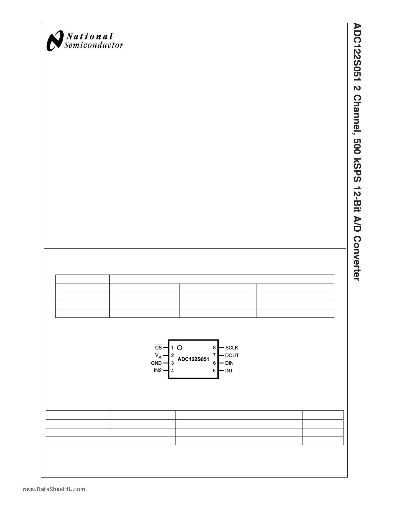
Connection Diagram
Ordering Information
Order Code
ADC122S051CIMM
ADC122S051CIMMX
ADC122S051EVAL
Temperature Range
−40˚C to +85˚C
−40˚C to +85˚C
TRI-STATE® is a trademark of National Semiconductor Corporation
QSPI™ and SPI™ are trademarks of Motorola, Inc.
© 2005 National Semiconductor Corporation DS201064
20106405
Description
8-Lead MSOP Package
8-Lead MSOP Package, Tape & Reel
Evaluation Board
Top Mark
X06C
X06C
www.national.com
1 page 
ADC122S051 Timing Specifications
The following specifications apply for VA = +2.7V to 5.25V, GND = 0V, fSCLK = 3.2 MHz to 8 MHz, fSAMPLE = 2w0w0wk.SDPaStatSoh5e0e0t4U.com
kSPS, CL = 35 pF, Boldface limits apply for TA = TMIN to TMAX: all other limits TA = 25˚C.
Symbol
Parameter
Conditions
Typical
Limits
(Note 7)
Units
tCSU
tCLH
tEN
tACC
tSU
tH
tCH
tCL
tDIS
Setup Time SCLK High to CS Falling Edge
Hold time SCLK Low to CS Falling Edge
Delay from CS Until DOUT active
Data Access Time after SCLK Falling Edge
Data Setup Time Prior to SCLK Rising Edge
Data Valid SCLK Hold Time
SCLK High Pulse Width
SCLK Low Pulse Width
CS Rising Edge to DOUT High-Impedance
(Note 10)
(Note 10)
VA = +3.0V
VA = +5.0V
VA = +3.0V
VA = +5.0V
VA = +3.0V
VA = +5.0V
VA = +3.0V
VA = +5.0V
Output Falling
Output Rising
VA = +3.0V
VA = +5.0V
VA = +3.0V
VA = +5.0V
−3.5
−0.5
+4.5
+1.5
+4
+2
+14.5
+13
+3
+3
0.5 x
tSCLK
0.5 x
tSCLK
1.8
1.3
1.0
1.0
10 ns (min)
10
30
30
10
10
0.3 x
tSCLK
0.3 x
tSCLK
ns (min)
ns
(max)
ns
(max)
ns (min)
ns (min)
ns (min)
ns (min)
ns
20
(max)
Note 1: Absolute Maximum Ratings indicate limits beyond which damage to the device may occur. Operating Ratings indicate conditions for which the device is
functional, but do not guarantee specific performance limits. For guaranteed specifications and test conditions, see the Electrical Characteristics. The guaranteed
specifications apply only for the test conditions listed. Some performance characteristics may degrade when the device is not operated under the listed test
conditions.
Note 2: All voltages are measured with respect to GND = 0V, unless otherwise specified.
Note 3: When the input voltage at any pin exceeds the power supply (that is, VIN < GND or VIN > VA), the current at that pin should be limited to 10 mA. The 20
mA maximum package input current rating limits the number of pins that can safely exceed the power supplies with an input current of 10 mA to two. The Absolute
Maximum Rating specification does not apply to the VA pin. The current into the VA pin is limited by the Analog Supply Voltage specification.
Note 4: The absolute maximum junction temperature (TJmax) for this device is 150˚C. The maximum allowable power dissipation is dictated by TJmax, the
junction-to-ambient thermal resistance (θJA), and the ambient temperature (TA), and can be calculated using the formula PDMAX = (TJmax − TA)/θJA. The values
for maximum power dissipation listed above will be reached only when the device is operated in a severe fault condition (e.g. when input or output pins are driven
beyond the power supply voltages, or the power supply polarity is reversed). Obviously, such conditions should always be avoided.
Note 5: Human body model is 100 pF capacitor discharged through a 1.5 kΩ resistor. Machine model is 220 pF discharged through zero ohms
Note 6: Reflow temperature profiles are different for lead-free and non-lead-free packages.
Note 7: Tested limits are guaranteed to National’s AOQL (Average Outgoing Quality Level).
Note 8: This is the frequency range over which the electrical performance is guaranteed. The device is functional over a wider range which is specified under
Operating Ratings.
Note 9: Datasheet min/max specification limits are guaranteed by design, test, or statistical analysis.
Note 10: Clock may be in any state (high or low) when CS is asserted, with the restrictions on setup and hold time given by tCSU and tCLH.
5 www.national.com
5 Page 
Typical Performance Characteristics TA = +25˚C, fSAMPLE = 200 kSPS to 500 kSPS, fSCLK = 3.2
MHz to 8 MHz, fIN = 40.2 kHz unless otherwise stated. (Continued)
www.DataSheet4U.com
SNR vs. Input Frequency
THD vs. Input Frequency
SNR vs. Temperature
20106433
THD vs. Temperature
20106438
SFDR vs. Supply
20106434
SINAD vs. Supply
20106439
20106440
11
20106445
www.national.com
11 Page | ||
| Páginas | Total 19 Páginas | |
| PDF Descargar | [ Datasheet ADC122S051.PDF ] | |
Hoja de datos destacado
| Número de pieza | Descripción | Fabricantes |
| ADC122S051 | 2 Channel- 500 kSPS 12-Bit A/D Converter | National Semiconductor |
| ADC122S051 | 2 Channel 200 ksps to 500 ksps 12-Bit A/D Converter (Rev. E) | Texas Instruments |
| ADC122S051Q-Q1 | ADC122S051 2 Channel 200 ksps to 500 ksps 12-Bit A/D Converter (Rev. E) | Texas Instruments |
| Número de pieza | Descripción | Fabricantes |
| SLA6805M | High Voltage 3 phase Motor Driver IC. |
Sanken |
| SDC1742 | 12- and 14-Bit Hybrid Synchro / Resolver-to-Digital Converters. |
Analog Devices |
|
DataSheet.es es una pagina web que funciona como un repositorio de manuales o hoja de datos de muchos de los productos más populares, |
| DataSheet.es | 2020 | Privacy Policy | Contacto | Buscar |