|
|
|
PDF W364M72V-XSBX Data sheet ( Hoja de datos )
| Número de pieza | W364M72V-XSBX | |
| Descripción | 64Mx72 Synchronous DRAM | |
| Fabricantes | White Electronic Designs Corporation | |
| Logotipo | ||
Hay una vista previa y un enlace de descarga de W364M72V-XSBX (archivo pdf) en la parte inferior de esta página. Total 16 Páginas | ||
|
No Preview Available !
White Electronic Designs
W364M72V-XSBX
www.DataSheet4UA.cDoVmANCED*
64Mx72 Synchronous DRAM
FEATURES
High Frequency = 100, 125MHz
Package:
• 219 Plastic Ball Grid Array (PBGA), 32 x 25mm
3.3V ±0.3V power supply for core and I/Os
Fully Synchronous; all signals registered on positive
edge of system clock cycle
Internal pipelined operation; column address can be
changed every clock cycle
Internal banks for hiding row access/precharge
Programmable Burst length 1,2,4,8 or full page
8,192 refresh cycles
Commercial, Industrial and Military Temperature
Ranges
Organized as 64M x 72
Weight: W364M72V-XSBX - TBD grams typical
* This product is under development, is not qualified or characterized and is subject to
change or cancellation without notice.
BENEFITS
66% SPACE SAVINGS
Reduced part count from 9 to 1
Reduced I/O count
• 55% I/O Reduction
Reduced trace lengths for lower parasitic
capacitance
Suitable for hi-reliability applications
Laminate interposer for optimum TCE match
GENERAL DESCRIPTION
The 512MByte (4.5Gb) SDRAM is a high-speed CMOS,
dynamic random-access, memory using 9 chips containing
512M bits. Each chip is internally configured as a quad-
bank DRAM with a synchronous interface. Each of the
chip’s 134,217,728-bit banks is organized as 8,192 rows
by 2,048 columns by 8 bits.
Read and write accesses to the SDRAM are burst oriented;
accesses start at a selected location and continue for a
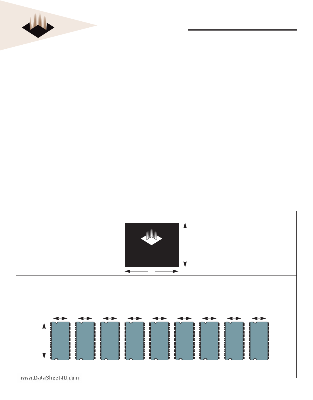
ACTUAL SIZE
White Electronic Designs
W364M72V-XSBX
25
Area = 800mm2
32
I/O Count = 219 Balls
SAVINGS – Area: 66% – I/O Count: 55%
Discrete Approach
11.9 11.9 11.9 11.9 11.9 11.9 11.9 11.9 11.9
22.3 54
TSOP
54
TSOP
54
TSOP
54
TSOP
54
TSOP
54
TSOP
54
TSOP
54
TSOP
54
TSOP
Area: 9 x 265mm2 = 2,385mm2
January 2005
Rev. 1
I/O Count: 9 x 54 pins = 486 pins
1 White Electronic Designs Corporation • (602) 437-1520 • www.wedc.com
1 page 
White Electronic Designs
W364M72V-XSBX
www.DataSheet4UA.cDoVmANCED
All inputs and outputs are LVTTL compatible. SDRAMs offer
substantial advances in DRAM operating performance,
including the ability to synchronously burst data at a high
data rate with automatic column-address generation,
the ability to interleave between internal banks in order
to hide precharge time and the capability to randomly
change column addresses on each clock cycle during a
burst access.
FUNCTIONAL DESCRIPTION
Read and write accesses to the SDRAM are burst oriented;
accesses start at a selected location and continue for
a programmed number of locations in a programmed
sequence. Accesses begin with the registration of an
ACTIVE command which is then followed by a READ or
WRITE command. The address bits registered coincident
with the ACTIVE command are used to select the bank and
row to be accessed (BA0 and BA1 select the bank, A0-12
select the row). The address bits (A0-9, A11) registered
coincident with the READ or WRITE command are used to
select the starting column location for the burst access.
Prior to normal operation, the SDRAM must be initialized.
The following sections provide detailed information
covering device initialization, register definition, command
descriptions and device operation.
INITIALIZATION
SDRAMs must be powered up and initialized in a predefined
manner. Operational procedures other than those specified
may result in undefined operation. Once power is applied
to VCC and VCCQ (simultaneously) and the clock is stable
(stable clock is defined as a signal cycling within timing
constraints specified for the clock pin), the SDRAM
requires a 100µs delay prior to issuing any command
other than a COMMAND INHIBIT or a NOP. Starting at
some point during this 100µs period and continuing at
least through the end of this period, COMMAND INHIBIT
or NOP commands should be applied.
Once the 100µs delay has been satisfied with at least
one COMMAND INHIBIT or NOP command having been
applied, a PRECHARGE command should be applied. All
banks must be precharged, thereby placing the device in
the all banks idle state.
Once in the idle state, two AUTO REFRESH cycles must be
performed. After the AUTO REFRESH cycles are complete,
the SDRAM is ready for Mode Register programming.
Because the Mode Register will power up in an unknown
state, it should be loaded prior to applying any operational
command.
REGISTER DEFINITION
MODE REGISTER
The Mode Register is used to define the specific mode
of operation of the SDRAM. This definition includes the
selec-tion of a burst length, a burst type, a CAS latency,
an operating mode and a write burst mode, as shown in
Figure 3. The Mode Register is programmed via the LOAD
MODE REGISTER command and will retain the stored
information until it is programmed again or the device
loses power.
Mode register bits M0-M2 specify the burst length, M3
specifies the type of burst (sequential or interleaved),
M4-M6 specify the CAS latency, M7 and M8 specify the
operating mode, M9 specifies the WRITE burst mode,
and M10 and M11 are reserved for future use. Address
A12 (M12) is undefined but should be driven LOW during
loading of the mode register.
The Mode Register must be loaded when all banks are
idle, and the controller must wait the specified time before
initiating the subsequent operation. Violating either of these
requirements will result in unspecified operation.
BURST LENGTH
Read and write accesses to the SDRAM are burst oriented,
with the burst length being programmable, as shown
in Figure 3. The burst length determines the maximum
number of column locations that can be accessed for a
given READ or WRITE command. Burst lengths of 1, 2, 4
or 8 locations are available for both the sequential and the
interleaved burst types, and a full-page burst is available
for the sequential type. The full-page burst is used in
conjunction with the BURST TERMINATE command to
generate arbitrary burst lengths.
Reserved states should not be used, as unknown operation
or incompatibility with future versions may result.
When a READ or WRITE command is issued, a block of
columns equal to the burst length is effectively selected.
All accesses for that burst take place within this block,
meaning that the burst will wrap within the block if a
boundary is reached. The block is uniquely selected by
A1-9, A11 when the burst length is set to two; by A2-9,
A11 when the burst length is set to four; and by A3-9, A11
when the burst length is set to eight. The remaining (least
significant) address bit(s) is (are) used to select the starting
location within the block. Full-page bursts wrap within the
page if the boundary is reached.
January 2005
Rev. 1
5 White Electronic Designs Corporation • (602) 437-1520 • www.wedc.com
5 Page 
White Electronic Designs
W364M72V-XSBX
www.DataSheet4UA.cDoVmANCED
DC ELECTRICAL CHARACTERISTICS AND OPERATING CONDITIONS (NOTES 1, 6)
VCC, VCCQ = +3.3V ± 0.3V; -55°C ≤ TA ≤ +125°C
Parameter/Condition
Symbol
Min
Max Units
Supply Voltage
Input High Voltage: Logic 1; All inputs (21)
Input Low Voltage: Logic 0; All inputs (21)
Input Leakage Current: Any input 0V ≤ VIN ≤ VCC (All other pins not under test = 0V)
Input Leakage Address Current (All other pins not under test = 0V)
Output Leakage Current: I/Os are disabled; 0V ≤ VOUT ≤ VCCQ
Output Levels:
Output High Voltage (IOUT = -4mA)
Output Low Voltage (IOUT = 4mA)
VCC,VCCQ
3
3.6
V
VIH 2 VCC + 0.3 V
VIL -0.3 0.8
V
II 10 10 µA
II -45 45 µA
IOZ -5 5 µA
VOH 2.4
–
V
VOL – 0.4 V
ICC SPECIFICATIONS AND CONDITIONS (NOTES 1,6,11,13)
VCC, VCCQ = +3.3V ± 0.3V; -55°C ≤ TA ≤ +125°C
Parameter/Condition
Symbol
Max
-125 -100
Operating Current: Active Mode;
Burst = 2; Read or Write; tRC = tRC (min); CAS latency = 3 (3, 18, 19)
Standby Current: Active Mode; CKE = HIGH; CS# = HIGH;
All banks active after tRCD met; No accesses in progress (3, 12, 19)
Operating Current: Burst Mode; Continuous burst;
Read or Write; All banks active; CAS latency = 3 (3, 18, 19)
ICC1 990 900
ICC3 405 405
ICC4 1,035 990
Self Refresh Current: CKE ≤ 0.2V (Commercial and Industrial Temperature: -40°C to + 85°C) (27)
ICC7 54
54
Units
mA
mA
mA
mA
January 2005
Rev. 1
11 White Electronic Designs Corporation • (602) 437-1520 • www.wedc.com
11 Page | ||
| Páginas | Total 16 Páginas | |
| PDF Descargar | [ Datasheet W364M72V-XSBX.PDF ] | |
Hoja de datos destacado
| Número de pieza | Descripción | Fabricantes |
| W364M72V-XSBX | 64Mx72 Synchronous DRAM | White Electronic Designs Corporation |
| Número de pieza | Descripción | Fabricantes |
| SLA6805M | High Voltage 3 phase Motor Driver IC. |
Sanken |
| SDC1742 | 12- and 14-Bit Hybrid Synchro / Resolver-to-Digital Converters. |
Analog Devices |
|
DataSheet.es es una pagina web que funciona como un repositorio de manuales o hoja de datos de muchos de los productos más populares, |
| DataSheet.es | 2020 | Privacy Policy | Contacto | Buscar |